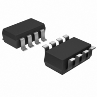
AD5171BRJ10-RL7 Analog Devices Inc, AD5171BRJ10-RL7 Datasheet - Page 5

AD5171BRJ10-RL7
Manufacturer Part Number
AD5171BRJ10-RL7
Description
IC DGTL POT OTP 10K SOT23-8
Manufacturer
Analog Devices Inc
Datasheet
1.AD5171BRJZ10-R7.pdf
(24 pages)
Specifications of AD5171BRJ10-RL7
Taps
64
Resistance (ohms)
10K
Number Of Circuits
1
Temperature Coefficient
35 ppm/°C Typical
Memory Type
Non-Volatile
Interface
I²C, 2-Wire Serial
Voltage - Supply
2.7 V ~ 5.5 V
Operating Temperature
-40°C ~ 125°C
Mounting Type
Surface Mount
Package / Case
SOT-23-8
Resistance In Ohms
10K
Number Of Elements
1
# Of Taps
64
Resistance (max)
10KOhm
Power Supply Requirement
Single
Interface Type
Serial (2-Wire/I2C)
Single Supply Voltage (typ)
3/5V
Dual Supply Voltage (typ)
Not RequiredV
Single Supply Voltage (min)
2.7V
Single Supply Voltage (max)
5.5V
Dual Supply Voltage (min)
Not RequiredV
Dual Supply Voltage (max)
Not RequiredV
Operating Temp Range
-40C to 125C
Operating Temperature Classification
Automotive
Mounting
Surface Mount
Pin Count
8
Lead Free Status / RoHS Status
Contains lead / RoHS non-compliant
For Use With
AD5171EVAL - BOARD EVAL FOR AD5171
Lead Free Status / RoHS Status
Not Compliant, Contains lead / RoHS non-compliant
Available stocks
Company
Part Number
Manufacturer
Quantity
Price
Part Number:
AD5171BRJ10-RL7
Manufacturer:
ADI/亚德诺
Quantity:
20 000
TIMING CHARACTERISTICS: 5 kΩ, 10 kΩ, 50 kΩ, AND 100 kΩ
V
Table 2.
Parameter
INTERFACE TIMING CHARACTERISTICS (APPLY TO ALL PARTS
1
2
3
Typical specifications represent average readings at 25°C and V
Guaranteed by design; not subject to production test.
All dynamic characteristics use V
DD
SCL Clock Frequency
t
t
t
t
t
t
t
t
t
t
OTP Program Time
BUF
HD;STA
LOW
HIGH
SU;STA
HD;DAT
SU;DAT
F
R
SU;STO
= 3 V to 5 V ± 10%, V
Fall Time of Both SDA and SCL Signals
Rise Time of Both SDA and SCL Signals
Bus Free Time Between Start and Stop
Low Period of SCL Clock
High Period of SCL Clock
Setup Time for Start Condition
Hold Time (Repeated Start)
Data Setup Time
Setup Time for Stop Condition
Data Hold Time
SDA
SCL
A
DD
= V
= 5 V.
P
DD
t
, V
1
B
S
= 0 V, −40°C < T
t
2
t
8
t
3
t
8
DD
Figure 3. Interface Timing Diagram
= 5 V.
A
< +125°C, unless otherwise noted.
t
9
2, 3
Rev. D | Page 5 of 24
)
t
4
Symbol
f
t
t
t
t
t
t
t
t
t
t
t
t
SCL
1
2
3
4
5
6
7
8
9
10
11
9
t
5
Conditions
After this period, the
first clock pulse is generated
t
6
t
7
P
Min
1.3
0.6
1.3
0.6
0.6
0.1
0.6
t
10
Typ
400
1
Max
400
50
0.9
0.3
0.3
AD5171
Unit
kHz
μs
μs
μs
μs
μs
μs
μs
μs
μs
μs
ms


