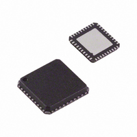
AD5405YCPZ Analog Devices Inc, AD5405YCPZ Datasheet - Page 16

AD5405YCPZ
Manufacturer Part Number
AD5405YCPZ
Description
IC DAC DUAL 12BIT MULT 40-LFCSP
Manufacturer
Analog Devices Inc
Datasheet
1.AD5405YCPZ.pdf
(24 pages)
Specifications of AD5405YCPZ
Data Interface
Parallel
Settling Time
80ns
Number Of Bits
12
Number Of Converters
2
Voltage Supply Source
Single Supply
Power Dissipation (max)
50µW
Operating Temperature
-40°C ~ 125°C
Mounting Type
Surface Mount
Package / Case
40-LFCSP
Resolution (bits)
12bit
Sampling Rate
21.3MSPS
Input Channel Type
Parallel
Supply Voltage Range - Analogue
2.5V To 5.5V
Supply Current
500nA
Digital Ic Case Style
CSP
Lead Free Status / RoHS Status
Lead free / RoHS Compliant
For Use With
EVAL-AD5405EB - BOARD EVAL FOR AD5405
Lead Free Status / RoHS Status
Lead free / RoHS Compliant, Lead free / RoHS Compliant
Available stocks
Company
Part Number
Manufacturer
Quantity
Price
Company:
Part Number:
AD5405YCPZ
Manufacturer:
Analog Devices Inc
Quantity:
1 779
Company:
Part Number:
AD5405YCPZ
Manufacturer:
Infineon
Quantity:
45
AD5405
V
DIVIDER OR PROGRAMMABLE GAIN ELEMENT
Current-steering DACs are very flexible and lend themselves to
many applications. If this type of DAC is connected as the
feedback element of an op amp and R
resistor, as shown in Figure 37, the output voltage is inversely
proportional to the digital input fraction, D.
For D = 1 − 2
As D is reduced, the output voltage increases. For small
values of the digital fraction D, it is important to ensure that
the amplifier does not saturate and that the required accuracy is
met. For example, an 8-bit DAC driven with the binary code 0x10
(0001 0000)—that is, 16 decimal—in the circuit of Figure 37
should cause the output voltage to be 16 times V
th
weight in the range of 15.5/256 to 16.5/256 so that the possible
output voltage is in the range of 15.5 V
of 3%, even though the DAC itself has a maximum error of 0.2%.
DAC leakage current is also a potential err
circuits. The leakage current m
opposite current supplied from
IN
e DAC has a linearity specification of ±0.5 LSB, D can have a
NOTES
1. SIMILAR CONFIGURATION FOR DAC B.
2. C1 PHASE COMPENSATION (1pF TO 2pF) MA
IF A1 IS A HIGH SPEED AMPLIFIER.
V
R1
OUT
NOTES
1. ADDITIONAL PINS OMITTED FOR CLARITY.
V
Figure 37. Current-Steering DAC Used as a Divider or
V
=
IN
REF
Figure 36. Increasing Gain of Current Output DAC
−
−n
A
V
, the output voltage is
IN
V
GND
V
I
I
OUT
OU
12-BIT
DD
DD
DAC
D
T
Programmable Gain Element
2A
1A
R
=
FB
A V
−
R
V
GND
V
I
FB
I
OUT
OUT
DD
IN
DD
A
1A
2A
(
1
ust be counterbalanced by an
the op amp through the DAC.
−
V
C
REF
2
1
−
n
A
FB
)
IN
Y BE REQUIRED
A is used as the input
to 16.5 V
or source in divider
R3
R2
V
OUT
IN
GAIN = R2 + R3
. However, if
IN
R1 = R2R3
—a
V
R2 + R3
OUT
n error
R2
Rev. B | Page 16 of 24
Because only a fraction, D, of the current into the V
is routed to the I
follows:
where R is the DAC resistance at the V
For a DAC leakage current of 10 nA, R = 10 kΩ, and a gain (that
is, 1/D) of 16, the error voltage is 1.6 mV.
REFERENCE SELECTION
When selecting a reference for use with the AD54xx series of
current output DACs, pay attention to the reference’s output
voltage te
only affects the full-scale error, but also can affect the linearity
(INL and DNL) performance. The reference temperature coef-
ficient should be consistent with the system accuracy specifica
tions. For example, an 8-bit sy
specification to within 1 LSB over the temperature range 0°C to
50°C dictates that the maximum system drift with temperature
should be less than 78 ppm/°C. A 12-bit system with the same
temperature range to overall specification within 2 LSBs requires
a maximum drift of 10 ppm/°C. Choosing a precision reference
with low output temperature coefficient minimizes this error
source.
Table 7 lists some references available from Analog Devices that
are suitable for use with this range of current output DACs.
AMPLIFIER SELECTION
The primary requirement for the current-steering mode is an
amplifier with low input bias currents and low input offset
voltage. Because of the code-dependent output resistance of th
DAC, the input offset voltage of an op amp is multiplied by the
variable gain of the circuit. A change in this noise gain betw
two adjacent digital fractions produces a step change in t
output voltage due to the amplifier’s input offset voltage.
output voltage change is superimposed on the desired chan
output between the two codes and gives rise to a differential
linearity error, which, if large enough, could cause the DAC
be nonmonotonic
The input bias current of an op amp also generates an offset at
the voltage output as a result of the bias current flowing in the
feedback resistor, R
enough to prevent significant errors in 12-bit applications.
Common-mode rejection of the op amp is important in
voltage-switching circuits, because it produces a code-
dependent error at the voltage output of the circuit. Most
op amps have adequate common-mode rejection for use at
12-bit resolution.
Provided that the DAC switches are driven from true wideband,
low impedance sources (V
Output Error Voltage Due to DAC Leakage = (Leakage × R)/D
mperature coefficient specification. This parameter not
OUT
.
FB
1 terminal, the output voltage changes as
. Most op amps have input bias currents low
IN
and AGND), they settle quic
stem required to hold its overall
REF
terminal.
REF
termina
he
This
kly.
ge in
een
to
e
-
l


