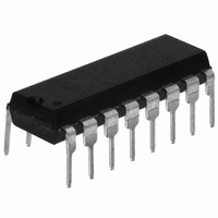
AD7943BNZ Analog Devices Inc, AD7943BNZ Datasheet - Page 14

AD7943BNZ
Manufacturer Part Number
AD7943BNZ
Description
IC DAC 12BIT MULT SRL 16DIP
Manufacturer
Analog Devices Inc
Datasheet
1.AD7943BNZ.pdf
(16 pages)
Specifications of AD7943BNZ
Data Interface
Serial
Settling Time
600ns
Number Of Bits
12
Number Of Converters
1
Voltage Supply Source
Single Supply
Power Dissipation (max)
25µW
Operating Temperature
-40°C ~ 85°C
Mounting Type
Through Hole
Package / Case
16-DIP (0.300", 7.62mm)
Resolution (bits)
12bit
Sampling Rate
1.7MSPS
Input Channel Type
Serial
Supply Voltage Range - Analogue
3V To 5.5V, 4.5V To 5.5V
Supply Current
5µA
Digital Ic Case Style
DIP
Lead Free Status / RoHS Status
Lead free / RoHS Compliant
Available stocks
Company
Part Number
Manufacturer
Quantity
Price
Company:
Part Number:
AD7943BNZ
Manufacturer:
SSOUSA
Quantity:
739
AD7943/AD7945/AD7948
BIPOLAR OPERATION
(Four-Quadrant Multiplication)
Figure 15 shows the standard connection diagram for bipolar
operation of the AD7943, AD7945 and AD7948. The coding is
offset binary as shown in Table IV. When V
the circuit performs four-quadrant multiplication. Resistors R1
and R2 are for gain error adjustment and are not needed in
many applications where the device gain error specifications are
adequate. To maintain the gain error specifications, resistors
R3, R4 and R5 should be ratio matched to 0.01%.
Suitable dual amplifiers for use with Figure 15 are the OP270
(low noise, low bandwidth, 15 kHz), the AD712 (medium
bandwidth, 200 kHz) or the AD827 (wide bandwidth, 1 MHz).
Table Digital Input
MSB
1111 1111 1111
1000 0000 0001
1000 0000 0000
0111 1111 1111
0000 0000 0001
0000 0000 0000
NOTE
Nominal LSB size for the circuit of Figure 15 is given by: V
V
IN
R1 20
Figure 15. Bipolar Operation (Four-Quadrant
Multiplication)
V
REF
NOTES
1. ONLY ONE DAC IS SHOWN FOR CLAIRITY.
2. DIGITAL INPUT CONNECTIONS ARE OMITTED.
3. C1 PHASE COMPENSATION (5 – 15pF) MAY BE REQUIRED
WHEN USING HIGH SPEED AMPLIFIER, A1.
LSB
Table IV. Bipolar (Offset Binary) Code
AD7943/45/48
DAC
RFB
R2 10
AGND
I
I
OUT1
OUT2
Analog Output
(V
+V
+V
+V
–V
–V
–V
OUT
REF
REF
REF
REF
REF
REF
SIGNAL GROUND
C1
(1/2048)
(2047/2048)
(2048/2048) = –V
as Shown in Figure 15)
(2047/2048)
(1/2048)
(0/2048) = 0
R4 20k
A1
IN
10k
R3
is an ac signal,
REF
(1/2048).
20k
R5
A2
REF
V
OUT
–14–
SINGLE SUPPLY APPLICATIONS
The “-B” versions of the devices are specified and tested for
single supply applications. Figure 16 shows the recommended
circuit for operation with a single +5 V to +3.3 V supply. The
I
applied to the V
0s loaded to the DAC) to 2.46 V (all 1s loaded). With 2.45 V
applied to the V
0s loaded) to 0.01 V (all 1s loaded). It is important when con-
sidering INL in a single-supply system to realize that most
single-supply amplifiers cannot sink current and maintain zero
volts at the output. In Figure 16, with V
quired sink current is 200 A. The minimum output voltage
level is 10 mV. Op amps like the OP295 are capable of main-
taining this level while sinking 200 A.
Figure 16 shows the I
by an amplifier. This is to maintain the bias voltage at 1.23 V
as the impedance seen looking into the I
This impedance is code dependent and varies from infinity (all
0s loaded in the DAC) to about 6 k minimum. The AD589
has a typical output resistance of 0.6
drive the terminals directly. However, this will cause a typical
linearity degradation of 0.2 LSBs. If this is unacceptable then
the buffer amplifier is necessary. Figure 9 shows the typical
linearity performance of the AD7943/AD7945/AD7948 when
used as in Figure 16 with V
OUT2
and AGND terminals are biased to 1.23 V. Thus, with 0 V
V
IN
V
REF
Figure 16. Single Supply System
REF
REF
V
DD
terminal, the output will go from 1.23 V (all
terminal, the output will go from 1.23 V (all
AD7943/45/48
AD589
5.6k
OUT2
DGND
+3.3V
DAC
RFB
+5V
and AGND terminals being driven
DD
SIGNAL GROUND
set at +3.3 V and V
A1
AGND
I
I
OUT1
OUT2
and it can be used to
REF
OUT2
C1
= 2.45 V the re-
A1
terminal changes.
A1: OP295
AD822
OP283
REF
V
= 0 V.
OUT
REV. B


