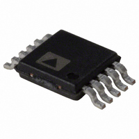
AD5664RBRMZ-3 Analog Devices Inc, AD5664RBRMZ-3 Datasheet - Page 18

AD5664RBRMZ-3
Manufacturer Part Number
AD5664RBRMZ-3
Description
IC DAC NANO 16BIT 1.25V 10-MSOP
Manufacturer
Analog Devices Inc
Series
nanoDAC™r
Specifications of AD5664RBRMZ-3
Data Interface
Serial
Settling Time
4µs
Number Of Bits
16
Number Of Converters
4
Voltage Supply Source
Single Supply
Power Dissipation (max)
6.6mW
Operating Temperature
-40°C ~ 105°C
Mounting Type
Surface Mount
Package / Case
10-MSOP, Micro10™, 10-uMAX, 10-uSOP
Resolution (bits)
16bit
Sampling Rate
220kSPS
Input Channel Type
Serial
Supply Current
950µA
Digital Ic Case Style
SOP
No. Of Pins
10
Lead Free Status / RoHS Status
Lead free / RoHS Compliant
For Use With
EVAL-AD5664REBZ - BOARD EVALUATION FOR AD5664R
Lead Free Status / RoHS Status
Lead free / RoHS Compliant, Lead free / RoHS Compliant
Available stocks
Company
Part Number
Manufacturer
Quantity
Price
Part Number:
AD5664RBRMZ-3
Manufacturer:
ADI/亚德诺
Quantity:
20 000
AD5624/AD5664
LDAC FUNCTION
The AD5624/AD5664 DACs have double-buffered interfaces
consisting of two banks of registers: input registers and DAC
registers. The input registers are connected directly to the input
shift register and the digital code is transferred to the relevant
input register on completion of a valid write sequence. The
DAC registers contain the digital code used by the resistor
strings.
The double-buffered interface is useful if the user requires
simultaneous updating of all DAC outputs. The user can write
to three of the input registers individually and then write to the
remaining input register and update all DAC registers, the
outputs update simultaneously. Command 010 is reserved for
this software LDAC.
Access to the DAC registers is controlled by the LDAC
function. The LDAC registers contain two modes of operation
for each DAC channel. The DAC channels are selected by
setting the bits of the 4-bit LDAC register (DB3, DB2, DB1, and
DB0). Command 110 is reserved for setting up the LDAC
register. When the LDAC bit register is set low, the
corresponding DAC registers are latched and the input
registers can change state without affecting the contents of the
Table 13. 24-Bit Input Shift Register Contents for LDAC Setup Command for the AD5624/AD5664
DB23 to
DB22
(MSB)
x
Don’t Care
DB21
1
Command bits (C2 to C0)
DB20
1
DB19
0
DB18
x
Address bits (A3 to A0); don’t care
DB17
x
Rev. 0 | Page 18 of 24
DB16
x
DAC registers. When the LDAC bit register is set high,
however, the DAC registers become transparent and the
contents of the input registers are transferred to them on the
falling edge of the 24
an LDAC hardware pin tied permanently low for the selected
DAC channel, that is, synchronous update mode. See Table 12
for the LDAC register mode of operation. See Table 13 for
contents of the input shift register during the LDAC register set-
up command.
This flexibility is useful in applications where the user wants to
update select channels simultaneously, while the rest of the
channels update synchronously.
Table 12. LDAC Register Mode of Operation
Load DAC Register
LDAC Bits
(DB3 to DB0)
0
1
DB15 to
DB4
x
Don’t
cares
th
SCLK pulse. This is equivalent to having
LDAC Mode of Operation
Normal operation (default), DAC register
update is controlled by write command.
The DAC registers are updated after new
data is read in on the falling edge of the
24
DB3
DacD
Set bit to 0 or 1 for required mode of
operation on respective channel
th
SCLK pulse.
DB2
DacC
DB1
DacB
DB0
(LSB)
DacA


