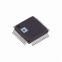
AD9767ASTZ Analog Devices Inc, AD9767ASTZ Datasheet

AD9767ASTZ
Specifications of AD9767ASTZ
Available stocks
Related parts for AD9767ASTZ
AD9767ASTZ Summary of contents
Page 1
FEATURES 14-bit dual transmit DAC 125 MSPS update rate SFDR and IMD: 82 dBc Gain and offset matching: 0.1% Fully independent or single resistor gain control Dual-port or interleaved data On-chip 1.2 V reference 3.3 V operation ...
Page 2
AD9767 TABLE OF CONTENTS Features .............................................................................................. 1 Applications....................................................................................... 1 General Description ......................................................................... 1 Functional Block Diagram .............................................................. 1 Product Highlights ........................................................................... 1 Revision History ............................................................................... 2 Specifications..................................................................................... 3 DC Specifications ......................................................................... 3 Dynamic Specifications ............................................................... 4 Digital Specifications ................................................................... 5 ...
Page 3
SPECIFICATIONS DC SPECIFICATIONS AVDD = 3 DVDD = 3 MIN MAX Table 1. Parameter RESOLUTION 1 DC ACCURACY Integral Linearity Error (INL 25° ...
Page 4
AD9767 DYNAMIC SPECIFICATIONS AVDD = 3 DVDD = 3 MIN MAX terminated, unless otherwise noted. Table 2. Parameter DYNAMIC PERFORMANCE Maximum Output Update Rate (f ) CLK ...
Page 5
DIGITAL SPECIFICATIONS AVDD = 3 DVDD = 3 MIN MAX Table 3. Parameter DIGITAL INPUTS Logic 1 Voltage @ DVDD = 5 V Logic 1 @ DVDD ...
Page 6
AD9767 ABSOLUTE MAXIMUM RATINGS Table 4. With Respect Parameter to Rating AVDD ACOM −0 +6.5 V DVDD DCOM −0 +6.5 V ACOM DCOM −0 AVDD DVDD −6 +6.5 V MODE, ...
Page 7
PIN CONFIGURATION AND FUNCTION DESCRIPTIONS DB13P1 (MSB) Table 6. Pin Function Descriptions Pin No. Name PORT1 15, 21 DCOM1, DCOM2 16, 22 DVDD1, DVDD2 17 WRT1/IQWRT 18 CLK1/IQCLK 19 CLK2/IQRESET 20 WRT2/IQSEL PORT2 37 ...
Page 8
AD9767 TYPICAL PERFORMANCE CHARACTERISTICS AVDD = 3 DVDD = 3 Nyquist, unless otherwise noted. 90 5MSPS 25MSPS 80 125MSPS 70 60 65MSPS (MHz) OUT Figure 4. SFDR ...
Page 9
A (dBFS) OUT Figure 10. Single-Tone SFDR vs OUT OUT 90 1MHz/5MSPS 85 2MHz/10MSPS 80 75 5MHz/25MSPS 70 65 13MHz/65MSPS ...
Page 10
AD9767 1MHz OUT 10MHz OUT 25MHz OUT 40MHz OUT 60MHz OUT 50 45 –60 –40 – TEMPERATURE (°C) Figure 16. SFDR ...
Page 11
TERMINOLOGY Linearity Error or Integral Nonlinearity (INL) Linearity error is defined as the maximum deviation of the actual analog output from the ideal output, determined by a straight line drawn from zero to full scale. Differential Nonlinearity (DNL) DNL is ...
Page 12
AD9767 THEORY OF OPERATION FSADJ1 R 1 SET REFIO 2kΩ 0.1µF FSADJ2 R 2 SET 2kΩ AD9767 1.2V REF WRT1/ GAINCTRL IQWRT DVDD 50Ω DCOM RETIMED CLOCK OUTPUT* LECROY 9210 PULSE GENERATOR Figure 21. Basic AC Characterization Test Setup for ...
Page 13
The full-scale output current of each DAC is regulated by separate reference control amplifiers and can be set from via an external resistor (R ), connected to the full SET scale adjust (FSADJ) pin. The ...
Page 14
AD9767 The two current outputs typically drive a resistive load directly or via a transformer coupling is required, I are directly connected to matching resistive loads (R are tied to analog common (ACOM). Note that R the equivalent ...
Page 15
The digital interface is implemented using an edge triggered master/slave latch. The DAC outputs are updated following either the rising edge or every other rising edge of the clock, depending on whether dual or interleaved mode is being used. The ...
Page 16
AD9767 Timing specifications for interleaved mode are shown in Figure 28 and Figure 29 DATA IN IQSEL IQWRT IQCLK OUTA OR I OUTB *APPLIES TO FALLING EDGE OF IQCLK/IQWRT AND ...
Page 17
TIME OF DATA CHANGE RELATIVE TO RISING CLOCK EDGE (ns) Figure 31. SNR vs. Clock Placement @ MHz and f OUT SLEEP MODE ...
Page 18
AD9767 APPLYING THE AD9767 OUTPUT CONFIGURATIONS The following sections illustrate some typical output configurations for the AD9767. Unless otherwise noted mA. For applications requiring the optimum dynamic per- formance, a differential output configuration is suggested. A differential output ...
Page 19
SINGLE-ENDED, UNBUFFERED VOLTAGE OUTPUT Figure 38 shows the AD9767 configured to provide a unipolar output range of approximately 0.5 V for a doubly terminated 50 Ω cable because the nominal full-scale current ( ...
Page 20
AD9767 at 250 kHz. To calculate the PSRR for a given R the units of PSRR are converted from A/V to V/V, adjust the curve in Figure 40 by the scaling factor 20 × log (RLOAD). For instance, if RLOAD ...
Page 21
APPLICATIONS VDSL APPLICATIONS USING THE AD9767 Very high frequency digital subscriber line (VDSL) technology is growing rapidly in applications requiring data transfer over relatively short distances. By using quadrature amplitude modulation (QAM) and transmitting the data in discrete multiple tones ...
Page 22
AD9767 EVALUATION BOARD GENERAL DESCRIPTION The AD9767- evaluation board for the AD9767 14-bit dual DAC. Careful attention to layout and circuit design, com- bined with a prototyping area, allow the user to easily and effectively evaluate the AD9767 ...
Page 23
RP3 RCOM 22Ω 1 DVDD RP5, 10Ω INP1 RP5, 10Ω INP2 RP5, 10Ω INP3 RP5, 10Ω INP4 ...
Page 24
AD9767 VAL 0.01µF 0.1µ DVDD DUTP1 1 DB13P1MSB MODE DUTP2 DB12P1 2 AVDD DUTP3 DB11P1 3 DB10P1 DUTP4 4 DUTP5 DB9P1 FSADJ1 5 DB8P1 DUTP6 6 REFIO DUTP7 DB7P1 GAINCTRL 7 ...
Page 25
Figure 48. Assembly, Top Side Figure 49. Assembly, Bottom Side Rev Page AD9767 ...
Page 26
AD9767 Figure 50. Layer 1, Top Side Figure 51. Layer 2, Ground Plane Rev Page ...
Page 27
Figure 52. Layer3, Power Plane Figure 53. Layer 4, Bottom Side Rev Page AD9767 ...
Page 28
... AD9767AST –40°C to +85°C AD9767ASTRL –40°C to +85°C 1 AD9767ASTZ –40°C to +85°C 1 AD9767ASTZRL –40°C to +85°C AD9767- Pb-free part. ©2006 Analog Devices, Inc. All rights reserved. Trademarks and registered trademarks are the property of their respective owners. C00620-0-10/06(C) 9 ...


