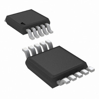
DAC104S085CIMM/NOPB National Semiconductor, DAC104S085CIMM/NOPB Datasheet

DAC104S085CIMM/NOPB
Specifications of DAC104S085CIMM/NOPB
DAC104S085CIMMTR
Available stocks
Related parts for DAC104S085CIMM/NOPB
DAC104S085CIMM/NOPB Summary of contents
Page 1
... DAC084S085 and the 12-bit DAC124S085. The DAC104S085 operates over the extended industrial tem- perature range of −40°C to +105°C. Pin Configuration SPI ™ trademark of Motorola, Inc. © 2008 National Semiconductor Corporation Features ■ Guaranteed Monotonicity ■ Low Power Operation ■ ...
Page 2
Ordering Information Order Numbers DAC104S085CISD DAC104S085CISDX DAC104S085CIMM DAC104S085CIMMX DAC104S085EVAL Block Diagram www.national.com Temperature Range ≤ ≤ −40°C T +105°C A ≤ ≤ LLP Tape-and-Reel −40°C T +105°C A ≤ ≤ −40°C T +105°C A ≤ ≤ MSOP Tape-and-Reel −40°C T ...
Page 3
Pin Descriptions LLP MSOP Symbol Pin No OUTA V 3 OUTB V 4 OUTC 5 V OUTD 6 GND 7 V REFIN SYNC 10 SCLK PAD 11 (LLP only) Type Supply ...
Page 4
... Absolute Maximum Ratings If Military/Aerospace specified devices are required, please contact the National Semiconductor Sales Office/ Distributors for availability and specifications. Supply Voltage Voltage on any Input Pin Input Current at Any Pin (Note 3) Package Input Current (Note 3) Power Consumption 25°C A ESD Susceptibility (Note 5) ...
Page 5
Symbol Parameter I Output Short Circuit Current (sink) OS Continuous Output I O Current (Note 10) C Maximum Load Capacitance Output Impedance OUT REFERENCE INPUT CHARACTERISTICS Input Range Minimum Input Range Maximum VREFIN Input Impedance LOGIC INPUT ...
Page 6
A.C. and Timing Characteristics Values shown in this table are design targets and are subject to change before product release. The following specifications apply for 1011. Boldface limits apply for T Symbol Parameter f SCLK Frequency SCLK ...
Page 7
Note 8: To guarantee accuracy required that V Note 9: Typical figures are 25°C, and represent most likely parametric norms. Test limits are guaranteed to National's AOQL (Average Outgoing Quality J Level). Note 10: This ...
Page 8
Transfer Characteristic Timing Diagrams www.national.com FIGURE 1. Input / Output Transfer Characteristic FIGURE 2. Serial Timing Diagram 8 20195305 20195306 ...
Page 9
Typical Performance Characteristics 1011, unless otherwise stated INL 3.0V A DNL 3.0V A INL/DNL REFIN REF A SCLK 20195352 20195354 = 3.0V A 20195356 9 ...
Page 10
INL/DNL SCLK INL/DNL vs Clock Duty Cycle at V INL/DNL vs Temperature at V www.national.com = 2.7V A 20195350 = 3.0V INL/DNL vs Clock Duty Cycle 20195324 = 3.0V INL/DNL vs Temperature at ...
Page 11
Zero Code Error vs 20195330 Zero Code Error vs. f SCLK 20195334 Zero Code Error vs. Temperature 20195336 Zero Code Error vs. V Zero Code Error vs. Clock Duty Cycle Full-Scale Error vs REFIN 20195331 20195335 ...
Page 12
Full-Scale Error vs. V Full-Scale Error vs. Clock Duty Cycle Supply Current vs. V www.national.com REFIN 20195332 Full-Scale Error vs. Temperature 20195338 Supply Current vs. Temperature A 20195344 12 Full-Scale Error vs. f SCLK 20195333 20195339 20195345 ...
Page 13
Glitch Response 20195346 Power-On Reset 13 20195347 www.national.com ...
Page 14
Functional Description 1.1 DAC SECTION The DAC104S085 is fabricated on a CMOS process with an architecture that consists of switches and resistor strings that are followed by an output buffer. The reference voltage is ex- ternally applied at V ...
Page 15
Normally, the SYNC line is kept low for at least 16 falling edges of SCLK and the DAC is updated on the 16th SCLK falling edge. However, if SYNC is brought high before the 16th falling edge, the data transfer ...
Page 16
LM4050 Available with accuracy of 0.44%, the LM4050 shunt refer- ence is also a good choice as a reference for the DAC104S085 available in 4.096V and 5V versions and comes in a space-saving 3-pin SOT23. FIGURE 6. ...
Page 17
An input capacitance of 1.0µF without any ESR requirement is required at the LP3985 input, while a 1.0µF ceramic ca- pacitor with an ESR requirement of 5mΩ to 500mΩ is required at the output. Careful interpretation and understanding of the ...
Page 18
DSP/MICROPROCESSOR INTERFACING Interfacing the DAC104S085 to microprocessors and DSPs is quite simple. The following guidelines are offered to hasten the design process. 2.3.1 ADSP-2101/ADSP2103 Interfacing Figure 10 shows a serial interface between the DAC104S085 and the ADSP-2101/ADSP2103. The DSP ...
Page 19
Physical Dimensions inches (millimeters) unless otherwise noted 10-Lead MSOP Order Numbers DAC104S085CIMM NS Package Number MUB10A 10-Lead LLP Order Numbers DAC104S085CISD NS Package Number SDA10A 19 www.national.com ...
Page 20
... For more National Semiconductor product information and proven design tools, visit the following Web sites at: Products Amplifiers www.national.com/amplifiers Audio www.national.com/audio Clock and Timing www.national.com/timing Data Converters www.national.com/adc Interface www.national.com/interface LVDS www.national.com/lvds Power Management www.national.com/power Switching Regulators www.national.com/switchers LDOs www.national.com/ldo LED Lighting www ...


