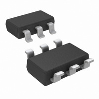
DAC101C081CIMK/NOPB National Semiconductor, DAC101C081CIMK/NOPB Datasheet - Page 3

DAC101C081CIMK/NOPB
Manufacturer Part Number
DAC101C081CIMK/NOPB
Description
DAC 10BIT MICROPWR I2C TSOT23-6
Manufacturer
National Semiconductor
Datasheet
1.DAC101C081CISDNOPB.pdf
(24 pages)
Specifications of DAC101C081CIMK/NOPB
Settling Time
3µs
Number Of Bits
10
Data Interface
I²C, Serial
Number Of Converters
1
Voltage Supply Source
Single Supply
Power Dissipation (max)
730µW
Operating Temperature
-40°C ~ 125°C
Mounting Type
Surface Mount
Package / Case
TSOT-23-6, TSOT-6
For Use With
DAC101C08XEB - BOARD EVALUATION FOR DAC101C08X
Lead Free Status / RoHS Status
Lead free / RoHS Compliant
Other names
DAC101C081CIMK
DAC101C081CIMK
DAC101C081CIMKTR
DAC101C081CIMK
DAC101C081CIMKTR
Available stocks
Company
Part Number
Manufacturer
Quantity
Price
Company:
Part Number:
DAC101C081CIMK/NOPB
Manufacturer:
TI
Quantity:
2 100
(LLP only)
Pin Descriptions
Package Pinouts Problem COL4
Symbol
MSOP-8
ADR0
ADR1
TSOT
V
GND
SDA
V
PAD
SCL
LLP
V
OUT
REF
A
Analog Output
Input/Output
Digital Input,
Digital Input,
Digital Input
V
three levels
three levels
OUT
1
6
8
Ground
Ground
Supply
Supply
Digital
Type
V
2
5
6
A
GND
3
4
5
Equivalent Circuit
SDA
4
3
4
3
SCL
5
2
3
Analog Output Voltage.
Power supply input. For the TSOT and LLP versions, this
supply is used as the reference. Must be decoupled to
GND.
Ground for all on-chip circuitry.
Serial Data bi-directional connection. Data is clocked into
or out of the internal 16-bit register relative to the clock
edges of SCL. This is an open drain data line that must be
pulled to the supply (V
Serial Clock Input. SCL is used together with SDA to
control the transfer of data in and out of the device.
Tri-state Address Selection Input. Sets the two Least
Significant Bits (A1 & A0) of the 7-bit slave address. (see
Table 1)
Tri-state Address Selection Input. Sets Bits A6 & A3 of the
7-bit slave address. (see Table 1)
Unbufferred reference voltage. For the MSOP-8, this
supply is used as the reference. V
and decoupled to GND.
Exposed die attach pad can be connected to ground or left
floating. Soldering the pad to the PCB offers optimal
thermal performance and enhances package self-
alignment during reflow.
ADR0
6
1
1
ADR1
N/A
N/A
2
Description
A
) by an external pull-up resistor.
V
N/A
N/A
REF
7
REF
must be free of noise
PAD (LLP only)
www.national.com
N/A
N/A
7


