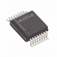
MAX5312EAE+ Maxim Integrated Products, MAX5312EAE+ Datasheet - Page 12

MAX5312EAE+
Manufacturer Part Number
MAX5312EAE+
Description
IC DAC 12BIT 5V/10V SER 16-SSOP
Manufacturer
Maxim Integrated Products
Datasheet
1.MAX5312EAE.pdf
(19 pages)
Specifications of MAX5312EAE+
Settling Time
10µs
Number Of Bits
12
Data Interface
Serial
Number Of Converters
1
Voltage Supply Source
Dual ±
Operating Temperature
-40°C ~ 85°C
Mounting Type
Surface Mount
Package / Case
16-SSOP
Number Of Dac Outputs
1
Resolution
12 bit
Interface Type
Serial (SPI)
Supply Voltage (max)
15.75 V
Supply Voltage (min)
10.8 V
Maximum Operating Temperature
+ 85 C
Mounting Style
SMD/SMT
Maximum Power Dissipation
571 mW
Minimum Operating Temperature
- 40 C
Supply Current
30 uA
Voltage Reference
External
Lead Free Status / RoHS Status
Lead free / RoHS Compliant
Power Dissipation (max)
-
Lead Free Status / Rohs Status
Lead free / RoHS Compliant
±10V, 12-Bit, Serial, Voltage-Output DAC
12
PIN
10
11
12
13
14
15
16
1
2
3
4
5
6
7
8
9
______________________________________________________________________________________
UNI/BIP
NAME
DGND
SGND
AGND
DOUT
SHDN
LDAC
SCLK
OUT
CLR
V
REF
V
DIN
V
CS
CC
DD
SS
Serial-Clock Input. Data is shifted from DIN into the internal register on the rising edge of SCLK. Data is
clocked out at DOUT on the falling edge of SCLK. SCLK is active only while CS is low.
S er i al - D ata Inp ut. D IN i s the d ata i np ut p or t for the ser i al i nter face. C l ock d ata i n on the r i si ng ed g e of S C LK.
Acti ve- Low C hi p - S el ect Inp ut. CS acti vates the ser i al i nter face. D r i ve CS l ow to i ni ti ate ser i al com m uni cati on.
Serial-Data Output. DOUT is the data output port for the serial interface. Data shifted into DIN appears at
DOUT 16.5 clock cycles later, valid on the falling edge of SCLK. DOUT is high impedance when CS is high.
Digital Ground
Digital Power Input. V
Active-Low Shutdown Input. SHDN places the device into low-power shutdown mode. When shut down
REF and DOUT are high impedance, drive SHDN low to place the device into shutdown mode.
Unipolar/Bipolar-Select Input. UNI/BIP selects unipolar or bipolar output. In unipolar mode, the analog
output range is 0 to (+2 x V
Drive UNI/BIP high for unipolar output. Drive UNI/BIP low for bipolar output. Dual supplies are required for
bipolar operation.
Analog Output. OUT is the output port for the DAC. Read OUT relative to SGND.
Signal Ground. SGND is the ground-reference node for the output amplifier’s internal feedback resistors.
Connect SGND directly to AGND. (See Figure 1.)
Analog Ground. AGND is the ground return for V
Negative Power Input. Bypass V
supply, connect V
External Reference Input. Apply an external reference voltage of +2V to +5.25V to REF to determine the
output voltage range. In unipolar mode, the output range is from 0 to (+2 x V
output range is from (-2 x V
Positive Power Input. Bypass V
Active-Low Clear Input. CLR clears input and DAC registers and resets the DAC output to 0V. Drive CLR
low to assert the clear condition.
Active-Low Load Input. Use LDAC to update the DAC register. LDAC is an asynchronous control input.
Drive low to force an update.
SS
to AGND.
CC
ranges from +2.7V to +5.5V. Bypass V
REF
REF
). In bipolar mode, the analog output range is (-2 x V
) to (+2 x V
DD
SS
with a 0.1µF and 1.0µF capacitor to AGND.
with a 0.1µF and 1.0µF capacitor to AGND. If operating with a single
REF
).
FUNCTION
DD
and V
SS
.
CC
with a 0.1µF and 1.0µF capacitor to
REF
). In bipolar mode, the
Pin Description
REF
) to (+2 x V
REF
).


