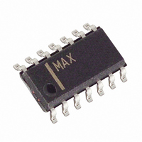
MAX531BCSD+ Maxim Integrated Products, MAX531BCSD+ Datasheet - Page 8

MAX531BCSD+
Manufacturer Part Number
MAX531BCSD+
Description
IC DAC V-OUT SRL 12BIT 5V 14SOIC
Manufacturer
Maxim Integrated Products
Datasheet
1.MAX531BCSD.pdf
(16 pages)
Specifications of MAX531BCSD+
Settling Time
25µs
Number Of Bits
12
Data Interface
Serial
Number Of Converters
1
Voltage Supply Source
Single Supply
Power Dissipation (max)
667mW
Operating Temperature
0°C ~ 70°C
Mounting Type
Surface Mount
Package / Case
14-SOIC (3.9mm Width), 14-SOL
Number Of Dac Outputs
1
Resolution
12 bit
Interface Type
Serial (SPI)
Supply Voltage (max)
5.25 V
Supply Voltage (min)
4.5 V
Maximum Operating Temperature
+ 70 C
Mounting Style
SMD/SMT
Maximum Power Dissipation
471 mW
Minimum Operating Temperature
0 C
Supply Current
260 uA
Voltage Reference
Internal
Lead Free Status / RoHS Status
Lead free / RoHS Compliant
+5V, Low-Power, Voltage-Output
Serial 12-Bit DACs
Figure 1. Timing Diagram
8
____________________Pin Description
MAX531
_______________________________________________________________________________________
10
11
12
13
14
1
2
3
4
5
6
7
8
9
DOUT
SCLK
DIN
CS
PIN
MAX538
MAX539
t
CSH0
—
—
—
—
—
—
1
2
3
4
5
6
7
8
t
DS
REFOUT
BIPOFF
NAME
DGND
AGND
DOUT
REFIN
VOUT
SCLK
CLR
V
RFB
DIN
V
CS
DD
SS
t
CSS
Bipolar Offset/Gain
Resistor
Serial Data Input
Clear. Asynchronously sets
DAC register to 000 hex.
Serial Clock Input
Chip Select, active low
Serial Data Output for
daisy-chaining
Digital Ground
Analog Ground
Reference Input
Reference Output,
2.048V
Negative Power Supply
DAC Output
Positive Power Supply
Feedback Resistor
t
DH
t
CH
FUNCTION
t
DO
t
CL
The MAX531/MAX538/MAX539 use an “inverted” R-2R
ladder network with a single-supply CMOS op amp to con-
vert 12-bit digital data to analog voltage levels (see
Functional Diagram) . The term “inverted” describes the
ladder network because the REFIN pin in current-output
DACs is the summing junction, or virtual ground, of an op
amp. However, such use would result in the output voltage
being the inverse of the reference voltage. The
MAX531/MAX538/MAX539’s topology makes the output
the same polarity as the reference input.
An internal reset circuit forces the DAC register to reset to
000 hex on power-up. Additionally, a clear CLR pin, when
held low, sets the DAC register to 000 hex. CLR operates
asynchronously and independently from the chip-select
(CS) pin.
The output buffer is a unity-gain stable, rail-to-rail output,
BiCMOS op amp. Input offset voltage and CMRR are
trimmed to achieve better than 12-bit performance.
Settling time is 25µs to 0.01% of final value. The settling
time is considerably longer when the DAC code is initially
set to 000 hex, because at this code the op amp is com-
pletely debiased. Start from code 001 hex if necessary.
The output is short-circuit protected and can drive a 2kΩ
load with more than 100pF load capacitance.
_______________Detailed Description
General DAC Discussion
t
CSH1
t
CS1
Buffer Amplifier
t
CSW


