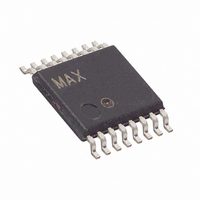
MAX5307EUE+ Maxim Integrated Products, MAX5307EUE+ Datasheet - Page 7

MAX5307EUE+
Manufacturer Part Number
MAX5307EUE+
Description
IC DAC 12BIT OCT LP SER 16-TSSOP
Manufacturer
Maxim Integrated Products
Datasheet
1.MAX5307EUE.pdf
(15 pages)
Specifications of MAX5307EUE+
Settling Time
5µs
Number Of Bits
12
Data Interface
Serial
Number Of Converters
8
Voltage Supply Source
Single Supply
Operating Temperature
-40°C ~ 85°C
Mounting Type
Surface Mount
Package / Case
16-TSSOP
Number Of Dac Outputs
8
Resolution
12 bit
Interface Type
Serial (SPI)
Supply Voltage (max)
5.5 V
Supply Voltage (min)
2.7 V
Maximum Operating Temperature
+ 85 C
Mounting Style
SMD/SMT
Minimum Operating Temperature
- 40 C
Supply Current
1.7 mA
Voltage Reference
External
Lead Free Status / RoHS Status
Lead free / RoHS Compliant
Power Dissipation (max)
-
Lead Free Status / Rohs Status
Lead free / RoHS Compliant
The MAX5306/MAX5307 are 12-bit, eight-channel, low-
power, voltage-output digital-to-analog converters
(DACs) that are easily addressed using a simple 3-wire
serial interface. These devices feature eight double-
buffered DACs using a common 16-bit serial to parallel
shift register, a power-on reset (POR) circuit and eight
output buffer amplifiers.
Figure 1 shows the block diagram of MAX5306/
MAX5307. The shift register converts a serial 16-bit
word to parallel data for each input register operating
with a clock rate of up to 15MHz. The 3-wire digital
interface to the shift register consist of chip-select (CS),
serial clock (SCLK), and data input (DIN). Serial data at
DIN is loaded on the falling edge of SCLK.
The eight double-buffered DACs consist of input and
DAC registers. The input registers are directly connect-
ed to the shift register and hold the result of the most
recent write operation. The eight 12-bit DAC registers
hold the current output code for the respective DAC.
Data can be transferred from the input registers to the
DAC registers by either the hardware interface (LDAC)
or by software command. The output of DACs are
buffered through eight Rail-to-Rail
The MAX5306 has a digital output (DOUT) which can
be used to daisy chain multiple devices on a single ser-
ial bus. The MAX5307 contains a hardware shutdown
(CLR) to clear all internal registers and power-down all
DACs.
Rail-to-Rail is a registered trademark of Nippon Motorola, Ltd.
5–12
PIN
13
14
15
16
1
2
3
4
Low-Power, Low-Glitch, Octal 12-Bit Voltage-
NAME
LDAC
DOUT
SCLK
OUT_
GND
CLR
REF
V
_______________________________________________________________________________________
DIN
CS
DD
Detailed Description
Serial Clock Input. Serial data is loaded on the falling edge of SCLK.
Serial Data Input
Load DAC. LDAC is an asynchronous active-low input that updates the DAC outputs
simultaneously. If LDAC is driven low, the DAC registers are transparent.
Reference Voltage Input
Analog Output Signal
Ground
Power Supply. Bypass V
Data Output (MAX5306). DOUT is updated on the falling edge of SCLK.
Asynchronous Clear DAC (MAX5307). Active-low input to clear all DACs and registers. Resets all
outputs to zero.
Chip-Select Input (active-low)
Output DACs with Serial Interface
®
op amps.
DD
to GND with a 0.1µF capacitor.
The MAX5306/MAX5307 require an external reference
such as the MAX6161 family. The reference voltage
range is from 0.8V to V
POR circuitry gives the DACs a defined state during
startup. At power-on, the DAC outputs reset to zero
through a 100kΩ resistor, providing additional safety for
applications that drive valves or other transducers that
need to be off at power-up.
The MAX5306/MAX5307 feature low digital feedthrough
and minimize glitch energy on MSB transitions. The 3-
wire SPI, QSPI, MICROWIRE and DSP-compatible seri-
al interface saves additional circuit board space .
The MAX5306/MAX5307 3-wire serial interface are
compatible with MICROWIRE, SPI, QSPI, and DSPs
(Figure 2 and Figure 3). The chip-select input (CS)
frames the serial data loading at DIN. Following CS’s
high-to-low transition, the data is shifted synchronously
and latched into the input register on each falling edge
of the serial clock input (SCLK). Each serial word is 16
bits, the first four bits are the control word followed by
12 data bits (MSB first) as shown in Table 1. The 12-bit
DAC code is unipolar binary with 1LSB = V
The serial input register transfers its contents to the
input registers after loading 16 bits of data and driving
CS high. CS must be brought high for a minimum of
20ns before the next write sequence since a write
FUNCTION
DD
.
Serial Interface
Pin Description
Configuration
REF
/4096.
7


