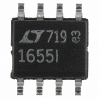
LTC1655IS8#PBF Linear Technology, LTC1655IS8#PBF Datasheet - Page 10

LTC1655IS8#PBF
Manufacturer Part Number
LTC1655IS8#PBF
Description
IC D/A CONV 16BIT R-R 8-SOIC
Manufacturer
Linear Technology
Datasheet
1.LTC1655CN8PBF.pdf
(16 pages)
Specifications of LTC1655IS8#PBF
Settling Time
20µs
Number Of Bits
16
Data Interface
Serial
Number Of Converters
1
Voltage Supply Source
Single Supply
Power Dissipation (max)
2.6mW
Operating Temperature
-40°C ~ 85°C
Mounting Type
Surface Mount
Package / Case
8-SOIC (3.9mm Width)
Number Of Channels
1
Resolution
16b
Conversion Rate
750KSPS
Interface Type
Serial (3-Wire, SPI, QSPI, Microwire)
Single Supply Voltage (typ)
5V
Dual Supply Voltage (typ)
Not RequiredV
Power Supply Requirement
Single
Output Type
Voltage
Integral Nonlinearity Error
±20LSB
Single Supply Voltage (min)
4.5V
Single Supply Voltage (max)
5.5V
Dual Supply Voltage (min)
Not RequiredV
Dual Supply Voltage (max)
Not RequiredV
Operating Temp Range
-40C to 85C
Operating Temperature Classification
Industrial
Mounting
Surface Mount
Pin Count
8
Package Type
SOIC N
Lead Free Status / RoHS Status
Lead free / RoHS Compliant
Available stocks
Company
Part Number
Manufacturer
Quantity
Price
APPLICATIONS
LTC1655/LTC1655L
Rail-to-Rail Output Considerations
In any rail-to-rail DAC, the output swing is limited to
voltages within the supply range.
If the DAC offset is negative, the output for the lowest
codes limits at 0V as shown in Figure 1b.
Similarly, limiting can occur near full-scale when the REF
pin is tied to V
NEGATIVE
10
OFFSET
VOLTAGE
OUTPUT
Figure 1. Effects of Rail-to-Rail Operation On a DAC Transfer Curve. (a) Overall Transfer Function (b) Effect of Negative
Offset for Codes Near Zero Scale (c) Effect of Positive Full-Scale Error for Input Codes Near Full Scale When V
0V
CC
/2. If V
U
REF
INPUT CODE
INFORMATION
(1b)
U
= V
CC
/2 and the DAC full-scale
VOLTAGE
W
OUTPUT
V
CC
0
V
U
REF
= V
CC
INPUT CODE
/2
32768
(1a)
error (FSE) is positive, the output for the highest codes
limits at V
can occur if V
Offset and linearity are defined and tested over the region
of the DAC transfer function where no output limiting can
occur.
CC
65535
as shown in Figure 1c. No full-scale limiting
REF
is less than (V
INPUT CODE
(1c)
CC
V
REF
– FSE)/2.
= V
CC
/2
REF
= V
V
OUTPUT
VOLTAGE
CC
CC
1655/55L F01
/2
POSITIVE
FSE


