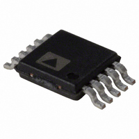
AD5623RBRMZ-5 Analog Devices Inc, AD5623RBRMZ-5 Datasheet - Page 21

AD5623RBRMZ-5
Manufacturer Part Number
AD5623RBRMZ-5
Description
IC DAC NANO 12BIT DUAL 10-MSOP
Manufacturer
Analog Devices Inc
Series
nanoDAC™r
Specifications of AD5623RBRMZ-5
Data Interface
Serial
Settling Time
3µs
Number Of Bits
12
Number Of Converters
2
Voltage Supply Source
Single Supply
Power Dissipation (max)
5mW
Operating Temperature
-40°C ~ 105°C
Mounting Type
Surface Mount
Package / Case
10-MSOP, Micro10™, 10-uMAX, 10-uSOP
Resolution (bits)
12bit
Sampling Rate
287kSPS
Input Channel Type
Serial
Supply Voltage Range - Analog
2.7V To 3.6V, 4.5V To 5.5V
Supply Current
800µA
Lead Free Status / RoHS Status
Lead free / RoHS Compliant
Available stocks
Company
Part Number
Manufacturer
Quantity
Price
Part Number:
AD5623RBRMZ-5
Manufacturer:
ADI/亚德诺
Quantity:
20 000
Part Number:
AD5623RBRMZ-5REEL
Manufacturer:
ADI/亚德诺
Quantity:
20 000
Company:
Part Number:
AD5623RBRMZ-5REEL7
Manufacturer:
TOSHIBA
Quantity:
5 000
At this stage, the SYNC line can be kept low or be brought high.
In either case, it must be brought high for a minimum of 15 ns
before the next write sequence, so that a falling edge of SYNC
can initiate the next write sequence.
Because the SYNC buffer draws more current when V
than it does when V
write sequences for even lower power operation. As mentioned
previously, it must, however, be brought high again just before
the next write sequence.
INPUT SHIFT REGISTER
The input shift register is 24 bits wide (see Figure 52). The first
two bits are don’t cares. The next three are Command Bit C2 to
Command Bit C0 (see Table 8), followed by the 3-bit DAC
Address A2 to DAC Address A0 (see Table 9), and, finally, the
16-, 14-, and 12-bit data-word.
The data-word comprises the 16-, 14-, and 12-bit input codes,
followed by zero, two, or four don’t care bits, for the AD5663R,
AD5643R, and AD5623R, respectively (see Figure 51, Figure 52,
and Figure 53). The data bits are transferred to the DAC register
on the 24th falling edge of SCLK.
SYNC
SCLK
DIN
DB23 (MSB)
DB23 (MSB)
DB23 (MSB)
SYNC HIGH BEFORE 24
X
X
X
DB23
INVALID WRITE SEQUENCE:
X
X
X
IN
= 0.8 V, SYNC should be idled low between
COMMAND BITS
COMMAND BITS
COMMAND BITS
C2
C2
C2
C1
C1
C1
TH
C0
C0
C0
FALLING EDGE
ADDRESS BITS
ADDRESS BITS
ADDRESS BITS
A2
A2
A2
DB0
A1
A1
A1
A0
A0
A0
Figure 51. AD5663R Input Shift Register Contents
Figure 52. AD5643R Input Shift Register Contents
Figure 53. AD5623R Input Shift Register Contents
D13
D15
D11
IN
D14
D12
D10
Figure 54. SYNC Interrupt Facility
= 2 V
D13
D11
D9
Rev. D | Page 21 of 32
D12
D10
D8
D11
D9
D7
DATA BITS
D10
DATA BITS
D8
D6
Table 8. Command Definition
C2
0
0
0
0
1
1
1
1
Table 9. Address Command
A2
0
0
0
0
1
SYNC INTERRUPT
In a normal write sequence, the SYNC line is kept low for at
least 24 falling edges of SCLK, and the DAC is updated on the
24th falling edge. However, if SYNC is brought high before the
24th falling edge, this acts as an interrupt to the write sequence.
The shift register is reset, and the write sequence is seen as
invalid. Neither an update of the DAC register contents nor a
change in the operating mode occurs (see
D9
D7
D5
VALID WRITE SEQUENCE, OUTPUT UPDATES
C1
0
0
1
1
0
0
1
1
D8
D6
D4
DATA BITS
A1
0
0
1
1
1
DB23
ON THE 24
C0
0
1
0
1
0
1
0
1
D7
D5
D3
AD5623R/AD5643R/AD5663R
D6
D4
D2
Command
Write to Input Register n
Update DAC Register n
Write to Input Register n, update all
(software LDAC)
Write to and update DAC Channel n
Power down DAC (power up)
Reset
LDAC register setup
Internal reference setup (on/off )
TH
0
1
0
1
1
A0
D5
D3
D1
FALLING EDGE
D2
D4
D0
D3
D1
X
DB0
ADDRESS (n)
DAC A
DAC B
Reserved
Reserved
All DACs
D0
D2
X
D1
DB0 (LSB)
DB0 (LSB)
DB0 (LSB)
X
X
Figure 54
D0
X
X
).


