AD5390BSTZ-5 Analog Devices Inc, AD5390BSTZ-5 Datasheet
AD5390BSTZ-5
Specifications of AD5390BSTZ-5
Available stocks


Related parts for AD5390BSTZ-5


AD5390BSTZ-5 Summary of contents
Page 1
FEATURES AD5390: 16-channel, 14-bit voltage output DAC AD5391: 16-channel, 12-bit voltage output DAC AD5392: 8-channel, 14-bit voltage output DAC Guaranteed monotonic INL: ±1 LSB max (AD5391) ±3 LSB max (AD5390-5/AD5392-5) ±4 LSB max (AD5390-3/AD5392-3) On-chip 1.25 V/2 ppm/°C ...
Page 2
AD5390/AD5391/AD5392 TABLE OF CONTENTS General Description ......................................................................... 3 AD5390-5/AD5391-5/AD5392-5 Specifications.......................... 4 AD5390-5/AD5391-5/AD5392-5 AC Characteristics................. 6 AD5390-3/AD5391-3/AD5392-3 Specifications.......................... 7 AD5390-3/AD5391-3/AD5392-3 AC Characteristics................. 9 Timing Characteristics: Serial SPI-, QSPI-, Microwire-, and DSP-Compatible Interface............................................................. 10 2 Timing Characteristics Serial Interface................................ 13 ...
Page 3
GENERAL DESCRIPTION The AD5390/AD5391 are complete single-supply, 16-channel, 14-bit and 12-bit DACs, respectively. The AD5392 is a complete single-supply, 8-channel, 14-bit DAC. Devices are available both in 64-lead LFCSP and 52-lead LQFP packages. All channels have an on-chip output amplifier ...
Page 4
AD5390/AD5391/AD5392 AD5390-5/AD5391-5/AD5392-5 SPECIFICATIONS 5.5 V; AGND = DGND = 0 V; REFIN = 2.5 V external All specifications unless otherwise noted. MIN ...
Page 5
Parameter LOGIC INPUTS (SCL, SDA Only Input High Voltage Input Low Voltage Input Leakage Current Input Hysteresis HYST C , Input Capacitance IN Glitch Rejection LOGIC OUTPUTS (BUSY, SDO) ...
Page 6
AD5390/AD5391/AD5392 AD5390-5/AD5391-5/AD5392-5 AC CHARACTERISTICS 5.5 V; AGND = DGND = Table 3. AD5390-5/AD5391-5/AD5392-5 AC Characteristics Parameter DYNAMIC PERFORMANCE Output Voltage Settling Time AD5390/AD5392 AD5391 ...
Page 7
AD5390-3/AD5391-3/AD5392-3 SPECIFICATIONS 5.5 V; AGND = DGND = 0 V; REFIN = 1.25 V external. All specifications otherwise noted. Table 4. Parameter ACCURACY Resolution Relative ...
Page 8
AD5390/AD5391/AD5392 Parameter Glitch Rejection Logic Outputs (BUSY, SDO) 2 Output Low Voltage Output High Voltage High Impedance Leakage Current High Impedance Output Capacitance Logic Output (SDA Output Low Voltage OL Three-State Leakage Current Three-State Output Capacitance POWER ...
Page 9
AD5390-3/AD5391-3/AD5392-3 AC CHARACTERISTICS 5.5 V; AGND = DGND = Table 5. AD5390-3/AD5391-3/AD5392-3 AC Characteristics Parameter DYNAMIC PERFORMANCE Output Voltage Settling Time AD5390/AD5392 AD5391 ...
Page 10
AD5390/AD5391/AD5392 TIMING CHARACTERISTICS: SERIAL SPI-, QSPI-, MICROWIRE-, AND DSP-COMPATIBLE INTERFACE 5 2 5.5 V; AGND = DGND = 0 V. All specifications Table 6. 3-Wire Serial ...
Page 11
SCLK SYNC DB23 DIN INPUT WORD FOR DAC N SDO UNDEFINED LDAC Figure 2. Serial Interface Timing Diagram (Daisy-Chain Mode) SCLK SYNC t 7 ...
Page 12
AD5390/AD5391/AD5392 SCLK SYNC DB23 DIN INPUT WORD SPECIFIES REGISTER TO BE READ SDO DB0 DB23' NOP CONDITION DB23 UNDEFINED SELECTED REGISTER DATA CLOCKED OUT Figure 4. Serial Interface Timing Diagram (Data Readback Mode) I 200µ ...
Page 13
TIMING CHARACTERISTICS: I Guaranteed by design and characterization, not production tested. DV All specifications unless otherwise noted. MIN MAX Table 7. 1 Parameter Limit MIN MAX F 400 SCL t 2.5 1 ...
Page 14
AD5390/AD5391/AD5392 ABSOLUTE MAXIMUM RATINGS Transient currents 100 mA do not cause SCR latch-up 25°C, unless otherwise noted. A Table 8. Parameter Rating AV to AGND −0 DGND −0.3 ...
Page 15
PIN CONFIGURATON AND FUNCTION DESCRIPTIONS PIN INDICATOR AD5390/ REF_GND 7 8 AD5391 REFOUT/REFIN SIGNAL_GND DAC_GND 1 TOP VIEW (Not to ...
Page 16
AD5390/AD5391/AD5392 Table 9. Pin Function Descriptions Mnemonic Function VOUTX Buffered Analog Outputs for Channel X. Each analog output is driven by a rail-to-rail output amplifier operating at a gain of 2. Each output is capable of driving an output load ...
Page 17
Mnemonic Function PD Power-Down (level-sensitive, active high). Used to place the device in low power mode, in which the device consumes 1 µA analog current and 20 µA digital current. In power-down mode, all internal analog circuitry is placed in ...
Page 18
AD5390/AD5391/AD5392 TERMINOLOGY Relative Accuracy Relative accuracy or endpoint linearity is a measure of the maximum deviation from a straight line passing through the endpoints of the DAC transfer function measured after adjusting for zero-scale error and full-scale error ...
Page 19
TYPICAL PERFORMANCE CHARACTERISTICS 2.0 1.5 1.0 0.5 0 –0.5 –1.0 –1.5 –2.0 0 4096 8192 INPUT CODE Figure 11. AD5390-5/AD5392-5 Typical INL Plot 2.0 1.5 1.0 0.5 0 –0.5 –1.0 –1.5 –2.0 0 4096 8192 INPUT CODE Figure 12. AD5390-3/AD5392-5 ...
Page 20
AD5390/AD5391/AD5392 WR BUSY VREF = 2. 25°C A EXITS SOFT PD TO MIDSCALE Figure 17. AD539x Exiting Soft Power-Down VOUT EXITS HARDWARE PD Figure 18. AD539x Exiting Hardware ...
Page 21
VREF = 1.25V 1.253 T = 25°C A 14ns/SAMPLE NUMBER 1.252 1 LSB CHANGE AROUND MIDSCALE GLITCH IMPULSE = 5nV-s 1.251 1.250 1.249 1.248 1.247 1.246 1.245 0 50 100 150 200 ...
Page 22
AD5390/AD5391/AD5392 25°C A DAC LOADED WITH MIDSCALE EXTERNAL REFERENCE Y AXIS = 5µV/DIV X AXIS = 100ms/DIV Figure 29. 0 Output Noise Plot ...
Page 23
FUNCTIONAL DESCRIPTION DAC ARCHITECTURE—GENERAL The AD5390/AD5391 are complete single-supply, 16-channel, voltage output DACs offering a resolution of 14 bits and 12 bits, respectively. The AD5392 is a complete single-supply, 8-channel, voltage output DAC offering 14-bit resolution. All devices are available ...
Page 24
AD5390/AD5391/AD5392 DATA DECODING—AD5390/AD5392 The AD5390/AD5392 contain an internal 14-bit data bus. The input data is decoded depending on the data loaded to the REG1 and REG0 bits of the input serial register. This is shown in Table 10. Data from ...
Page 25
INTERFACES The AD5390/AD5391/AD5392 contain a serial interface that can be programmed to be either DSP-, SPI-, and MICROWIRE compatible C-compatible. The SPI/ I the interface mode. To minimize both the power consumption of the device and ...
Page 26
AD5390/AD5391/AD5392 Standalone Mode By connecting the daisy-chain enable (DCEN) pin low, standalone mode is enabled. The serial interface works with both a continuous and a noncontinuous serial clock. The first falling edge of SYNC starts the write cycle and resets ...
Page 27
I C SERIAL INTERFACE The AD5390/AD5391/AD5392 products feature an I compatible 2-wire interface consisting of a serial data line (SDA) and a serial clock line (SCL). SDA and SCL facilitate communication between the DACs and the master at rates ...
Page 28
AD5390/AD5391/AD5392 WRITE OPERATION There are three specific modes in which data can be written to the AD539x family of DACs. 4-BYTE MODE When writing to the AD539x DACs, begin with an address byte (R/W = 0), after ...
Page 29
MODE The 3-byte mode lets the user update more than one channel in a write sequence without having to write the device address byte each time. The device address byte is required only once and subsequent channel updates require ...
Page 30
AD5390/AD5391/AD5392 2-BYTE MODE The 2-byte mode lets the user update channels sequentially following initialization of this mode. The device address byte is required only once and the address pointer is configured for autoincrement or burst mode. The user must begin ...
Page 31
AD539x ON-CHIP SPECIAL FUNCTION REGISTERS The AD539x family of parts contains a number of special function registers (SFRs) as shown in Table 22. SFRs are addressed with REG1 = 0 and REG0 = 0 and are decoded using Address Bits ...
Page 32
AD5390/AD5391/AD5392 Table 23. AD5390/AD5392 Channel Monitor Decoding REG1 REG0 ...
Page 33
CONTROL REGISTER WRITE Table 25 shows the control register contents for the AD5390 and the AD5392. Table 26 provides bit descriptions. Note that REG1 = REG0 = 0, A3–A0 = 1100, and DB13–DB0 contain the control register data. Table 25. ...
Page 34
AD5390/AD5391/AD5392 Table 27 shows the control register contents of the AD5391. Table 28 provides bit descriptions. Note that REG1 = REG0 = 0, A3–A0 = 1100, and DB13–DB0 contain the control register data. Table 27. AD5391 Control Register Contents MSB ...
Page 35
HARDWARE FUNCTIONS RESET FUNCTION Bringing the RESET line low resets the contents of all internal registers to their power-on reset state. RESET is a negative edge- sensitive input. The default corresponds full scale and c at zero ...
Page 36
AD5390/AD5391/AD5392 AD539x to PIC16C6x/7x The PIC16C6x/7x synchronous serial port (SSP) is configured as an SPI master with the clock polarity bit = 0. This is done by writing to the synchronous serial port control register (SSPCON). See the PIC16/17 Microcontroller ...
Page 37
APPLICATION INFORMATION POWER SUPPLY DECOUPLING In any circuit where accuracy is important, careful consideration of the power supply and ground return layout helps to ensure the rated performance. The printed circuit board on which the AD539x is mounted should be ...
Page 38
AD5390/AD5391/AD5392 Digital connections have been omitted for clarity. The AD539x contains an internal power-on reset circuit with brown- out time. If the power supply ramp rate exceeds 10 ms, the user should reset the AD539x as part ...
Page 39
Power Amplifier Control Multistage power amplifier designs require a large number of setpoints in the operation and control of the output stage. The AD539x are ideal for these applications because of their small size (LFCSP package) and the integration of ...
Page 40
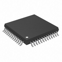
AD5390/AD5391/AD5392 OUTLINE DIMENSIONS PIN 1 INDICATOR 1.00 12° MAX 0.85 0.80 SEATING PLANE 1.45 1.40 1.35 0.15 SEATING 0.05 PLANE ROTATED 90° CCW 9.00 BSC SQ 0.60 MAX 48 TOP 8.75 VIEW BSC SQ 0.45 33 0.40 0.35 0.80 MAX ...
Page 41
ORDERING GUIDE Temperature Model Range AD5390BCP-3 −40°C to +85°C AD5390BCP-3-REEL −40°C to +85°C AD5390BCP-3-REEL7 −40°C to +85°C AD5390BCP-5 −40°C to +85°C AD5390BCP-5-REEL −40°C to +85°C AD5390BCP-5-REEL7 −40°C to +85°C AD5390BST-3 −40°C to +85°C AD5390BST-3-REEL −40°C to +85°C AD5390BST-5 −40°C to ...
Page 42
AD5390/AD5391/AD5392 NOTES Rev Page ...
Page 43
NOTES Rev Page AD5390/AD5391/AD5392 ...
Page 44
AD5390/AD5391/AD5392 NOTES Purchase of licensed components of Analog Devices or one of its sublicensed Associated Companies conveys a license for the purchaser under the Philips I Rights to use these components system, ...