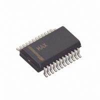
MAX5181BEEG+ Maxim Integrated Products, MAX5181BEEG+ Datasheet - Page 12

MAX5181BEEG+
Manufacturer Part Number
MAX5181BEEG+
Description
IC DAC 10BIT 40MHZ DUAL 24-QSOP
Manufacturer
Maxim Integrated Products
Datasheet
1.MAX5184ETG.pdf
(16 pages)
Specifications of MAX5181BEEG+
Settling Time
25µs
Number Of Bits
10
Data Interface
Parallel
Number Of Converters
1
Voltage Supply Source
Analog and Digital
Operating Temperature
-40°C ~ 85°C
Mounting Type
Surface Mount
Package / Case
24-QSOP
Number Of Dac Outputs
1
Resolution
10 bit
Interface Type
Parallel
Supply Voltage (max)
3.3 V
Supply Voltage (min)
2.7 V
Maximum Operating Temperature
+ 85 C
Mounting Style
SMD/SMT
Maximum Power Dissipation
762 mW
Minimum Operating Temperature
- 40 C
Supply Current
4.2 mA
Lead Free Status / RoHS Status
Lead free / RoHS Compliant
Power Dissipation (max)
-
Lead Free Status / Rohs Status
Lead free / RoHS Compliant
10-Bit, 40MHz, Current/Voltage-Output DACs
Figure 5a. Integral Nonlinearity
Figure 5c. Offset Error
The I/Q reconstruction system is completed by a quad-
rature modulator that combines the reconstructed com-
ponents with in-phase and quadrature carrier
frequencies and then sums both outputs to provide the
QAM signal.
Designing a traditional arbitrary waveform generator
(AWG) requires five major functional blocks (Figure 8a):
clock generator, counter, waveform memory, DAC for
waveform reconstruction, and output filter. The wave-
form memory contains the sequentially stored digital
replica of the desired analog waveforms. This memory
shares a common clock with the DAC.
12
______________________________________________________________________________________
7
6
5
4
3
2
1
0
3
2
1
0
Using the MAX5181/MAX5184 for
000
000
Arbitrary Waveform Generation
ACTUAL
OFFSET
POINT
001
IDEAL OFFSET
POINT
DIAGRAM
ACTUAL
010
001
DIGITAL INPUT CODE
DIGITAL INPUT CODE
AT STEP
001 (1/4 LSB )
011
OFFSET ERROR
(+1 1/4 LSB)
100
AT STEP
011 (1/2 LSB )
010
101
IDEAL DIAGRAM
110
011
111
For each clock cycle, a counter adds one count to the
address for the waveform memory. The memory then
loads the next value to the DAC, which generates an
analog output voltage corresponding to that data value.
A DAC output filter can either be a simple or complex
lowpass filter, depending on the AWG requirements for
waveform function and frequencies. The main limita-
tions of the AWG’s flexibility are DAC resolution and
dynamic performance, memory length, clock frequen-
cy, and the filter characteristics.
Although the MAX5181/MAX5184 offer high-frequency
operation and excellent dynamics, they are suitable for
relaxed requirements in resolution (10-bit AWGs). To
increase an AWG’s high-frequency accuracy, tempera-
Figure 5b. Differential Nonlinearity
Figure 5d. Gain Error
6
5
4
3
2
1
0
7
6
5
4
0
000
000
IDEAL DIAGRAM
100
001
GAIN ERROR
(-1 1/4 LSB)
IDEAL FULL-SCALE OUTPUT
DIGITAL INPUT CODE
DIGITAL INPUT CODE
010
101
1 LSB
011
DIFFERENTIAL
LINEARITY ERROR (+1/4 LSB)
DIFFERENTIAL LINEARITY
ERROR (-1/4 LSB)
100
110
FULL-SCALE
101
OUTPUT
ACTUAL
1 LSB
111


