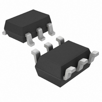
LTC2630CSC6-HZ8#TRMPBF Linear Technology, LTC2630CSC6-HZ8#TRMPBF Datasheet - Page 6

LTC2630CSC6-HZ8#TRMPBF
Manufacturer Part Number
LTC2630CSC6-HZ8#TRMPBF
Description
IC DAC 8BIT R-R SC70-6
Manufacturer
Linear Technology
Datasheet
1.LTC2630CSC6-LZ8TRMPBF.pdf
(20 pages)
Specifications of LTC2630CSC6-HZ8#TRMPBF
Settling Time
3.2µs
Number Of Bits
8
Data Interface
Serial
Number Of Converters
1
Voltage Supply Source
Single Supply
Power Dissipation (max)
480µW
Operating Temperature
0°C ~ 70°C
Mounting Type
Surface Mount
Package / Case
SC-70-6, SC-88, SOT-363
Number Of Channels
1
Resolution
8b
Interface Type
Serial (3-Wire, SPI, Microwire)
Single Supply Voltage (typ)
5V
Dual Supply Voltage (typ)
Not RequiredV
Power Supply Requirement
Single
Output Type
Voltage
Integral Nonlinearity Error
±0.5LSB
Single Supply Voltage (min)
4.5V
Single Supply Voltage (max)
5.5V
Dual Supply Voltage (min)
Not RequiredV
Dual Supply Voltage (max)
Not RequiredV
Operating Temp Range
0C to 70C
Operating Temperature Classification
Commercial
Mounting
Surface Mount
Pin Count
6
Package Type
SC-70
Lead Free Status / RoHS Status
Lead free / RoHS Compliant
Available stocks
Company
Part Number
Manufacturer
Quantity
Price
LTC2630
ELECTRICAL CHARACTERISTICS
temperature range, otherwise specifi cations are at T
LTC2630-HM12/-HM10/-HM8/-HZ12/-HZ10/-HZ8, LTC2630A-HM12/-HZ12 (V
6
SYMBOL PARAMETER
DC Performance
DNL
INL
ZSE
V
V
FSE
V
R
SYMBOL PARAMETER
V
PSR
I
Power Supply
V
I
I
Digital I/O
V
V
I
C
SC
CC
SD
LK
OS
OSTC
FSTC
OUT
CC
IH
IL
IN
OUT
Resolution
Monotonicity
Differential Nonlinearity V
Integral Nonlinearity
Zero Scale Error
Offset Error
V
Coeffi cient
Full Scale Error
Full Scale Voltage
Temperature
Coeffi cient
Load Regulation
DC Output Impedance V
DAC Output Span
Power Supply Rejection
Short Circuit Output Current (Note 6)
Power Supply Voltage
Supply Current (Note 7)
Supply Current in Power-Down Mode
(Note 7)
Digital Input High Voltage
Digital Input Low Voltage
Digital Input Leakage
Digital Input Capacitance
OS
Sinking
Sourcing
Temperature
CONDITIONS
V
V
V
V
V
V
V
V
Mid-Scale, –10mA ≤ I
Mid-Scale, –10mA ≤ I
CC
CC
CC
CC
CC
CC
CC
CC
CC
CC
C-Grade
I-Grade
H-Grade
= 5V, Internal Ref. (Note 4)
= 5V, Internal Ref. (Note 4)
= 5V, Internal Ref. (Note 4)
= 5V, Internal Ref., Code = 0
= 5V, Internal Ref. (Note 5)
= 5V, Internal Ref. (Note 5)
= 5V, Internal Ref.
= 5V, Internal Ref. (Note 10)
= 5V ±10%, Internal Ref.,
= 5V ±10%, Internal Ref.,
OUT
OUT
CONDITIONS
Supply as Reference
Internal Reference
V
V
For Specifi ed Performance
V
V
V
V
V
(Note 8)
CC
FS
CC
CC
CC
CC
IN
Zero Scale; V
Full Scale; V
≤ 10mA
≤ 10mA
= GND to V
= V
= 5V ±10%
= 5V, Supply as Reference
= 5V, Internal Reference
= 5V, C-Grade, I-Grade
= 5V, H-Grade
A
= 25°C. V
CC
= 5.5V
●
●
●
●
●
●
●
●
●
The
OUT
OUT
CC
MIN TYP MAX MIN TYP MAX MIN TYP MAX MIN TYP MAX
8
8
●
Shorted to GND
CC
Shorted to V
LTC2630-8
denotes the specifi cations which apply over the full operating
±0.05 ±0.5
±0.2 ±0.8
±10
±10
±10
0.006 0.01
0.1
= 4.5V to 5.5V, V
±0.5
±10
0.5
0.156
±0.5
±5
5
CC
FS
= 4.096V)
10
10
LTC2630-10
±10
±0.2 ±0.8
±10
±10
±10
0.025 0.04
0.1
OUT
±0.2
±0.5
●
●
●
●
●
●
●
●
●
●
●
0.5
unloaded unless otherwise specifi ed.
0.156
±0.5
±1
±5
5
MIN
4.5
2.4
12
12
LTC2630-12
±10
±0.2 ±0.8
±10
±10
±10
0.10 0.16
0.1
±0.5
0.5
±1
0V to 4.096
0V to V
0.36
0.36
TYP
–80
–28
180
200
27
0.156
±1
±2
±5
5
CC
12
12
LTC2630A-12
±0.5
±10
±0.2 ±0.8
±10
±10
±10
0.10 0.16
0.1
±0.5
0.5
MAX
–50
260
280
5.5
1.8
0.8
2.5
50
±1
5
0.156
±1
±1
±5
5
ppm/°C
ppm/°C
ppm/°C
UNITS
mV/°C
UNITS
%FSR
2630fe
LSB/
LSB
LSB
Bits
Bits
mA
mA
mV
mV
mA
dB
μA
μA
μA
μA
μA
pF
Ω
V
V
V
V
V


