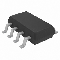
LTC2640HTS8-HM8#TRMPBF Linear Technology, LTC2640HTS8-HM8#TRMPBF Datasheet

LTC2640HTS8-HM8#TRMPBF
Specifications of LTC2640HTS8-HM8#TRMPBF
Available stocks
Related parts for LTC2640HTS8-HM8#TRMPBF
LTC2640HTS8-HM8#TRMPBF Summary of contents
Page 1
... Reset to Zero-Scale or Reset to Mid-Scale after power-up. L, LT, LTC and LTM are registered trademarks of Linear Technology Corporation. ThinSOT is a trademark of Linear Technology Corporation. All other trademarks are the property of their respective owners. Protected by U.S. Patents including 5396245, 5859606, 6891433, 6937178 and 7414561. ...
Page 2
LTC2640 ABSOLUTE MAXIMUM RATINGS (Notes 1, 2) Supply Voltage (V ) ................................... –0. CLR, CS/LD, REF_SEL, SCK, SDI ................. –0. REF ......................... –0.3V to Min(V OUT Operating Temperature Range LTC2640C ................................................ 0°C to ...
Page 3
ORDER INFORMATION LTC2640 A C TS8 – Consult LTC Marketing for information on non-standard lead based fi nish parts. For more information on lead free part marking, go to: For more information on tape and reel specifi cations, ...
Page 4
LTC2640 PRODUCT SELECTION GUIDE V WITH INTERNAL FS PART NUMBER PART MARKING* REFERENCE LTC2640A-LM12 LTDHV 2.5V • (4095/4096) LTC2640A-LZ12 LTDHW 2.5V • (4095/4096) LTC2640A-HM12 LTDHX 4.096V • (4095/4096) LTC2640A-HZ12 LTDHY 4.096V • (4095/4096) LTC2640-LM12 LTDHV 2.5V • (4095/4096) LTC2640-LM10 LTDHZ ...
Page 5
ELECTRICAL CHARACTERISTICS temperature range, otherwise specifi cations are at T LTC2640-LM12/-LM10/-LM8/-LZ12/-LZ10/-LZ8, LTC2640A-LM12/-LZ12 (V SYMBOL PARAMETER CONDITIONS DC Performance Resolution Monotonicity V = 3V, Internal Ref. (Note 4) CC DNL Differential V = 3V, Internal Ref. (Note 4) CC Nonlinearity INL ...
Page 6
LTC2640 ELECTRICAL CHARACTERISTICS temperature range, otherwise specifi cations are at T LTC2640-LM12/-LM10/-LM8/-LZ12/-LZ10/-LZ8, LTC2640A-LM12/-LZ12 (V SYMBOL PARAMETER Reference Input Input Voltage Range Resistance Capacitance I Reference Current, Power-Down Mode REF Reference Output Output Voltage Reference Temperature Coeffi cient Output Impedance Capacitive ...
Page 7
TIMING CHARACTERISTICS range, otherwise specifi cations are at T LTC2640-LM12/-LM10/-LM8/-LZ12/-LZ10/-LZ8, LTC2640A-LM12/-LZ12 (V SYMBOL PARAMETER t SDI Valid to SCK Setup 1 t SDI Valid to SCK Hold 2 t SCK High Time 3 t SCK Low Time 4 CS/LD Pulse ...
Page 8
LTC2640 ELECTRICAL CHARACTERISTICS temperature range, otherwise specifi cations are at T LTC2640-HM12/-HM10/-HM8/-HZ12/-HZ10/-HZ8, LTC2640A-HM12/-HZ12 (V SYMBOL PARAMETER V DAC Output Span OUT PSR Power Supply Rejection I Short-Circuit Output Current (Note 6) SC Sinking Sourcing Power Supply V Positive Supply Voltage ...
Page 9
ELECTRICAL CHARACTERISTICS temperature range, otherwise specifi cations are at T LTC2640-HM12/-HM10/-HM8/-HZ12/-HZ10/-HZ8, LTC2640A-HM12/-HZ12 (V SYMBOL PARAMETER e Output Voltage Noise Density n Output Voltage Noise TIMING CHARACTERISTICS range, otherwise specifi cations are at T LTC2640-HM12/-HM10/-HM8/-HZ12/-HZ10/-HZ8, LTC2640A-HM12/-HZ12 (V SYMBOL PARAMETER t SDI ...
Page 10
LTC2640 TYPICAL PERFORMANCE CHARACTERISTICS LTC2640-L12 (Internal Reference 2.5V) FS Integral Nonlinearity (INL) 1 0.5 0 –0.5 –1.0 0 1024 2048 3072 4095 CODE 2640 G01 INL vs Temperature 1 0.5 ...
Page 11
TYPICAL PERFORMANCE CHARACTERISTICS LTC2640-H12 (Internal Reference 4.096V) FS Integral Nonlinearity (INL) 1 0.5 0 –0.5 –1.0 0 1024 2048 3072 CODE 2640 G09 INL vs Temperature 1 0.5 INL (POS) ...
Page 12
LTC2640 TYPICAL PERFORMANCE CHARACTERISTICS LTC2640-10 Integral Nonlinearity (INL) 1 4.096V FS INTERNAL REF . 0.5 0 –0.5 –1.0 0 256 512 CODE LTC2640-8 Integral Nonlinearity (INL) 1 2.5V ...
Page 13
TYPICAL PERFORMANCE CHARACTERISTICS LTC2640 Gain Error 0.4 EXTERNAL REF . V = 2.5V REF 0.3 0.2 0.1 0.0 –0.1 –0.2 –0.3 –0.4 2.5 3 3 (V) CC 2640 G24 Mid-Scale-Glitch Impulse CS/LD 5V/DIV ...
Page 14
LTC2640 TYPICAL PERFORMANCE CHARACTERISTICS LTC2640 Multiplying Bandwidth 0 –2 –4 –6 –8 –10 –12 – REF(DC) – 0.2V REF(AC) P-P CODE = FULL SCALE –18 1k 10k 100k 1000k FREQUENCY (Hz) ...
Page 15
BLOCK DIAGRAMS SDI SCK 24-BIT SHIFT REGISTER CS/LD SDI SCK 24-BIT SHIFT REGISTER CS/LD LTC2640-Z V REF CC INTERNAL SWITCH REFERENCE CONTROL RESISTOR DECODE LOGIC DIVIDER DACREF INPUT DAC DAC REGISTER REGISTER CLR GND LTC2640-M V REF CC INTERNAL REFERENCE ...
Page 16
LTC2640 TIMING DIAGRAM SCK SDI CS/ Figure 1. Serial Interface Timing 2640 F01 2640fb ...
Page 17
OPERATION The LTC2640 is a family of single voltage-output DACs in 8-lead ThinSOT packages. Each DAC can operate rail- to-rail using an external reference, or with its full-scale voltage set by an integrated reference. 12 combinations of accuracy (12-, 10-, ...
Page 18
LTC2640 OPERATION Serial Interface The CS/LD input is level triggered. When this input is taken low, it acts as a chip-select signal, enabling the SDI and SCK buffers and the input shift register. Data (SDI input) is transferred at the ...
Page 19
OPERATION Power-Down Mode For power-constrained applications, the LTC2640’s power- down mode can be used to reduce the supply current whenever the DAC output is not needed. When in power- down, the buffer amplifi er, bias circuit, and reference circuit are ...
Page 20
LTC2640 OPERATION this effect than any other parts of this type; on the con- trary, it allows layout-based performance improvements to shine rather than limiting attainable performance with excessive internal resistance. Another technique for minimizing errors is to use a ...
Page 21
OPERATION LTC2640 2640fb 21 ...
Page 22
LTC2640 OPERATION OUTPUT VOLTAGE 0V NEGATIVE INPUT CODE OFFSET (b) Figure 4. Effects of Rail-to-Rail Operation on a DAC Transfer Curve (Shown for 12-Bits) (a) Overall Transfer Function (b) Effect of Negative Offset for Codes Near Zero (c) Effect of ...
Page 23
... JEDEC PACKAGE REFERENCE IS MO-193 Information furnished by Linear Technology Corporation is believed to be accurate and reliable. However, no responsibility is assumed for its use. Linear Technology Corporation makes no representa- tion that the interconnection of its circuits as described herein will not infringe on existing patent rights. TS8 Package ...
Page 24
... OUT Selectable External Ref. Mode, Rail-to-Rail Output, I www.linear.com ● 10V 0.1μ OUT V = ±5V OUT REF 0.1μF –10V 2640 TA03 2 C Interface Pins for Each DAC REF 2 C Interface LT 1108 REV B • PRINTED IN USA © LINEAR TECHNOLOGY CORPORATION 2008 2640fb ...


