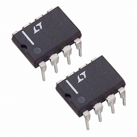
LTC1661CN8 Linear Technology, LTC1661CN8 Datasheet - Page 6

LTC1661CN8
Manufacturer Part Number
LTC1661CN8
Description
IC D/A CONV 10BIT MICRPWR 8-DIP
Manufacturer
Linear Technology
Datasheet
1.LTC1661CMS8PBF.pdf
(14 pages)
Specifications of LTC1661CN8
Settling Time
30µs
Number Of Bits
10
Data Interface
Serial
Number Of Converters
2
Voltage Supply Source
Single Supply
Power Dissipation (max)
260µW
Operating Temperature
0°C ~ 70°C
Mounting Type
Through Hole
Package / Case
8-DIP (0.300", 7.62mm)
Lead Free Status / RoHS Status
Contains lead / RoHS non-compliant
Available stocks
Company
Part Number
Manufacturer
Quantity
Price
Company:
Part Number:
LTC1661CN8#PBF
Manufacturer:
Linear Technology
Quantity:
1 787
Company:
Part Number:
LTC1661CN8#PBF
Manufacturer:
LTC
Quantity:
2 142
PIN FUNCTIONS
LTC1661
TYPICAL PERFORMANCE CHARACTERISTICS
CS/LD (Pin 1): Serial Interface Chip Select/Load Input.
When CS/LD is low, SCK is enabled for shifting data on
D
disabled and the operation(s) specified in the control code,
A3-A0, is (are) performed. CMOS and TTL compatible.
SCK (Pin 2): Serial Interface Clock Input. CMOS and TTL
compatible.
D
the D
edge of SCK. CMOS and TTL compatible.
6
IN
IN
(Pin 3): Serial Interface Data Input. Input word data on
into the register. When CS/LD is pulled high, SCK is
IN
pin is shifted into the 16-bit register on the rising
1.0
0.8
0.6
0.4
0.2
0
0
Supply Current
vs Logic Input Voltage
1
LOGIC INPUT VOLTAGE (V)
2
ALL DIGITAL INPUTS
SHORTED TOGETHER
3
4
1661 G10
5
REF (Pin 4): Reference Voltage Input. 0V ≤ V
V
The output range is
V
GND (Pin 7): System Ground.
OUT A
CC
0 ≤ V
(Pin 6): Supply Voltage Input. 2.7V ≤ V
, V
150
140
130
120
110
100
OUTA,
90
80
70
60
50
OUT B
–55 –35 –15
Supply Current vs Temperature
V
CODE = 1023
V
REF
(Pin 8, Pin 5): DAC Analog Voltage Outputs.
OUTB
= V
CC
TEMPERATURE (°C)
≤ V
V
V
V
V
5
CC
CC
CC
CC
= 5.5V
= 4.5V
= 3.6V
= 2.7V
REF
25
45
1023
1024
65
85 105 125
1661 G11
CC
REF
≤ 5.5V.
≤ V
CC
1661fa
.


