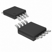
LTC1669IMS8 Linear Technology, LTC1669IMS8 Datasheet

LTC1669IMS8
Specifications of LTC1669IMS8
Available stocks
Related parts for LTC1669IMS8
LTC1669IMS8 Summary of contents
Page 1
... The LTC1669 is pin-for-pin compatible with the LTC1663. For SMBus-compatible designs, please refer to the LTC1663. L, LT, LTC and LTM are registered trademarks of Linear Technology Corporation. All other trademarks are the property of their respective owners ...
Page 2
... PLASTIC MSOP T = 125°C, θ = 150°C/W JMAX JA ORDER INFORMATION LEAD FREE FINISH TAPE AND REEL LTC1669CMS8#PBF LTC1669CMS8#TRPBF LTC1669IMS8#PBF LTC1669IMS8#TRPBF LTC1669-8CMS8#PBF LTC1669-8CMS8#TRPBF LTC1669-8IMS8#PBF LTC1669-8IMS8#TRPBF TAPE AND REEL (MINI) TAPE AND REEL LTC1669CS5#TRMPBF LTC1669CS5#TRPBF LTC1669-1CS5#TRMPBF LTC1669-1CS5#TRPBF TRM = 500 pieces. Consult LTC Marketing for parts specifi ed with wider operating temperature ranges. ...
Page 3
ELECTRICAL CHARACTERISTICS ture range, otherwise specifi cations are at T SYMBOL PARAMETER DAC Resolution Monotonicity DNL Differential Nonlinearity INL Integral Nonlinearity V Offset Error OS V Offset Error Temperature Coeffi cient OSTC FSE Full-Scale Error V DAC Output Span OUT ...
Page 4
LTC1669 ELECTRICAL CHARACTERISTICS ture range, otherwise specifi cations are at T SYMBOL PARAMETER Address Inputs AD0, AD1, AD2 (MSOP Only) I Address Pin Pull-Up Current UP V High Level Input Voltage IH V Low Level Input Voltage IL TIMING CHARACTERISTICS ...
Page 5
TYPICAL PERFORMANCE CHARACTERISTICS Integral Nonlinearity (INL) 1 REF CC 0 25°C A 0.6 0.4 0.2 0 –0.2 –0.4 –0.6 –0.8 –1.0 768 896 1024 0 28 156 384 512 640 CODE 1669 G01 ...
Page 6
LTC1669 PIN FUNCTIONS SDA (Pin 1, Pin 1 on SOT-23): Serial Data Bidirectional Pin. Data is shifted into the SDA pin and acknowledged by the SDA pin. High impedance pin while data is shifted in. Open-drain N-channel output during acknowledgment. ...
Page 7
DEFINITIONS Differential Nonlinearity (DNL): The difference between the measured change and the ideal 1LSB change for any two adjacent codes. The DNL error between any two codes is calculated as follows: DNL = (ΔV – LSB)/LSB OUT Where ΔV is ...
Page 8
LTC1669 TIMING DIAGRAM 8 1669fa ...
Page 9
APPLICATIONS INFORMATION Slave Address S = Start Condition Write Bit = Acknowledge Stop Condition Serial Digital Interface The LTC1669 communicates with a host (master) using the standard 2-wire interface. The ...
Page 10
LTC1669 APPLICATIONS INFORMATION Slave Address (SOT-23 Package) The slave address for the SOT-23 package has been factory programmed to be “0100 000” (LTC1669) and “0100 001” (LTC1669-1). If another address is required, please consult the factory. Command Byte 7 6 ...
Page 11
APPLICATIONS INFORMATION SYNC Address/Quick Command In addition to the slave address, the LTC1669 has an address that can be shared by other devices so that they may be updated synchronously. The address is called to the SYNC address and uses ...
Page 12
LTC1669 APPLICATIONS INFORMATION OUTPUT VOLTAGE 0V NEGATIVE INPUT CODE OFFSET (b) Figure 1. Effects of Rail-to-Rail Operation On a DAC Transfer Curve. (a) Overall Transfer Function (b) Effect of Negative Offset for Codes Near Zero Scale (c) Effect of Positive ...
Page 13
APPLICATIONS INFORMATION 3.9V TO 20V LTC1669 PIN NUMBERS IN PARENTHESES REFER TO MSOP PACKAGE LT1460S3 OUT + GND 0.1μF 0.01μ ( (4) SCL TO LTC1669 1 (1) μP SDA GND 2 ...
Page 14
LTC1669 PACKAGE DESCRIPTION 0.62 MAX 3.85 MAX 2.62 REF RECOMMENDED SOLDER PAD LAYOUT PER IPC CALCULATOR 0.20 BSC DATUM ‘A’ 0.30 – 0.50 REF NOTE: 1. DIMENSIONS ARE IN MILLIMETERS 2. DRAWING NOT TO SCALE 3. DIMENSIONS ARE INCLUSIVE OF ...
Page 15
... LEAD COPLANARITY (BOTTOM OF LEADS AFTER FORMING) SHALL BE 0.102mm (.004") MAX Information furnished by Linear Technology Corporation is believed to be accurate and reliable. However, no responsibility is assumed for its use. Linear Technology Corporation makes no representa- tion that the interconnection of its circuits as described herein will not infringe on existing patent rights. ...
Page 16
... V OUT0 CC 0.1μF CONTROL OUTPUT 1 0V ≤ V < V OUT1 CC 0.1μF CONTROL OUTPUT 15 0V ≤ V < V OUT15 CC 1669 TA06 DAC. Output Swings from GND to REF . REF OUT . 3-Wire Interface 1007 REV A • PRINTED IN USA © LINEAR TECHNOLOGY CORPORATION 2007 1669fa ...


