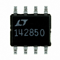
LTC1428CS8-50#PBF Linear Technology, LTC1428CS8-50#PBF Datasheet - Page 3

LTC1428CS8-50#PBF
Manufacturer Part Number
LTC1428CS8-50#PBF
Description
IC DAC 8BIT SINK OUT 8-SOIC
Manufacturer
Linear Technology
Datasheet
1.LTC1428CS8-50PBF.pdf
(8 pages)
Specifications of LTC1428CS8-50#PBF
Number Of Bits
8
Data Interface
Serial
Number Of Converters
1
Voltage Supply Source
Single Supply
Power Dissipation (max)
120µW
Operating Temperature
0°C ~ 70°C
Mounting Type
Surface Mount
Package / Case
8-SOIC (3.9mm Width)
Number Of Channels
1
Resolution
8b
Interface Type
SERIAL 1,2,3 WIRE
Single Supply Voltage (typ)
3.3V
Dual Supply Voltage (typ)
Not RequiredV
Power Supply Requirement
Single
Output Type
Current
Single Supply Voltage (min)
3V
Single Supply Voltage (max)
6.5V
Dual Supply Voltage (min)
Not RequiredV
Dual Supply Voltage (max)
Not RequiredV
Operating Temp Range
0C to 70C
Operating Temperature Classification
Commercial
Mounting
Surface Mount
Pin Count
8
Package Type
SOIC N
Resolution (bits)
8bit
Input Channel Type
Serial
Supply Current
130µA
Digital Ic Case Style
SOIC
No. Of Pins
8
Operating Temperature Range
0°C To +70°C
Msl
MSL 1 - Unlimited
Rohs Compliant
Yes
Lead Free Status / RoHS Status
Lead free / RoHS Compliant
Settling Time
-
Lead Free Status / Rohs Status
Compliant
Available stocks
Company
Part Number
Manufacturer
Quantity
Price
RECO
SYMBOL PARAMETER
Serial Interface
f
t
t
t
t
t
t
t
t
t
t
t
t
t
The
temperature range.
Note 1: Absolute Maximum Ratings are those values beyond which the life
of the device may be impaired.
TYPICAL PERFORMANCE CHARACTERISTICS
CLK
CKS
CSS
DV
DS
DH
DO
CKHI
CKLO
CSH
DZ
CKH
CSLO
CSHI
– 1.0
– 0.2
– 0.4
– 0.6
– 0.8
1.0
0.8
0.6
0.4
0.2
0
denotes specifications which apply over the full operating
0
DNL vs Code
V
V(I
T
A
CC
Clock Frequency
Setup Time, CLK Before CS
Setup Time, CS Before CLK
CS to D
D
D
CLK to D
CLK High Time
CLK Low Time
CLK Before CS
CS to D
CS Before CLK
CS Low Time
CS High Time
OUT
= 25 C
32
W W
IN
IN
= 3.3V
) = 2.5V
Setup Time Before CLK
Hold Time After CLK
64
OUT
OUT
E DED OPERATI G CO DITIO S
OUT
96
U
Valid
in Hi-Z
Valid
CODE
128 160
192 224 256
W
1428-50 G01
U
–0.2
–0.4
–0.6
–0.8
–1.0
U
1.0
0.8
0.6
0.4
0.2
0
0
INL vs Code
V
V(I
T
CC
A
32
OUT
= 25 C
= 3.3V
) = 2.5V
64
CONDITIONS
See Test Circuits
See Test Circuits
See Test Circuits
f
V
CLK
U
CLK
96
= 2MHz (Note 4)
= 0V
CODE
128 160
Note 2: Timing for all input signals is measured at 0.8V for a High-to-Low
transition and at 2V for a Low-to-High transition.
Note 3: Timing specifications are guaranteed by design but not tested.
Note 4: This is the minimum time required for valid data transfer.
U
192 224 256
1428-50 G02
V
CC
= 5V, unless otherwise specified. (Notes 2, 3)
– 0.5
– 1.0
– 1.5
– 2.0
2.0
1.5
1.0
0.5
0
Supply Voltage Rejection
1
V(I
T
A
4550
MIN
OUT
150
400
150
150
150
150
200
250
150
400
400
= 25 C
2
) = 2.5V
SUPPLY VOLTAGE (V)
3
LTC1428-50
TYP
4
MAX
400
400
2
5
6
1428-50 G03
UNITS
3
MHz
ns
ns
ns
ns
ns
ns
ns
ns
ns
ns
ns
ns
ns
ns
7


