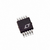
LTC2634IMSE-HMI8#TRPBF Linear Technology, LTC2634IMSE-HMI8#TRPBF Datasheet - Page 20

LTC2634IMSE-HMI8#TRPBF
Manufacturer Part Number
LTC2634IMSE-HMI8#TRPBF
Description
IC DAC 8BIT QUAD 2.5V 10-MSOP
Manufacturer
Linear Technology
Datasheet
1.LTC2634IMSE-LZ10PBF.pdf
(30 pages)
Specifications of LTC2634IMSE-HMI8#TRPBF
Settling Time
3.3µs
Number Of Bits
8
Data Interface
MICROWIRE™, Serial, SPI™
Number Of Converters
4
Voltage Supply Source
Single Supply
Power Dissipation (max)
1.8mW
Operating Temperature
-40°C ~ 85°C
Mounting Type
Surface Mount
Package / Case
10-MSOP Exposed Pad, 10-HMSOP, 10-eMSOP
Lead Free Status / RoHS Status
Lead free / RoHS Compliant
Available stocks
Company
Part Number
Manufacturer
Quantity
Price
LTC2634
operation
of CS/LD. The rising edge of CS/LD ends the data transfer
and causes the device to execute the command specified
in the 24-bit input sequence. The complete sequence is
shown in Figure 3a.
The command (C3-C0) and address (A3-A0) assignments
are shown in Tables 1 and 2. The first four commands
in Table 1 consist of write and update operation. A write
operation loads a 16-bit data word from the 24-bit shift
register into the input register of the selected DAC, n. An
Table 1. Command Codes
COMMAND*
*Command codes not shown are reserved and should not be used.
0
C3
0
0
0
0
0
0
0
0
1
Input Word (LTC2634-12)
Input Word (LTC2634-10)
Input Word (LTC2634-8)
C2
0
0
0
0
1
1
1
1
1
C1
C3
C3
C3
0
0
1
1
0
0
1
1
1
COMMAND
COMMAND
COMMAND
C2
C2
C2
C0
0
1
0
1
0
1
0
1
1
Write to Input Register n
Update (Power Up) DAC Register n
Write to Input Register n, Update (Power Up) All
Write to and Update (Power Up) DAC Register n
Power-Down DAC n
Power-Down Chip (All DACs and Reference)
Select Internal Reference (Power-Up Reference)
Select External Reference (Power-Down Internal
Reference)
No Operation
C1 C0
C1 C0
C1 C0
A3
A3
A3
ADDRESS
ADDRESS
ADDRESS
A2
A2
A2
A1
A1
A1
Figure 2. Command and Data Input Format
A0
A0
A0
MSB
MSB
MSB
D11
D9
D7
D10
D8
D6
D9
D7
D5
D8
D6
D4
update operation copies the data word from the input
register to the DAC register. Once copied into the DAC
register, the data word becomes the active 12-, 10- or
8-bit input code, and is converted to an analog voltage at
the DAC output. Write to and update combines the first
two commands. The update operation also powers up the
DAC if it had been in power-down mode. The data path
and registers are shown in the Block Diagram.
Table 2. Address Codes
ADDRESS (n)*
* Address codes not shown are reserved and should not be used.
A3
0
0
0
0
1
D7 D6
D5 D4
D3 D2
DATA (12 BITS + 4 DON’T CARE BITS)
DATA (10 BITS + 6 DON’T CARE BITS)
DATA (8 BITS + 8 DON’T CARE BITS)
A2
0
0
0
0
1
A1
D5 D4 D3 D2 D1 D0
D3 D2 D1 D0
D1 D0
0
0
1
1
1
LSB
A0
0
1
0
1
1
DAC A
DAC B
DAC C
DAC D
All DACs
X
LSB
X
X
X
LSB
X
X
X
X
X
X
X
X
X
X
X
2634 F02
X
X
X
2634fc


