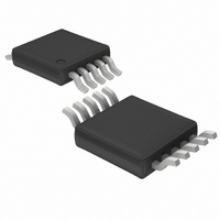
LTC2642IMS-12#PBF Linear Technology, LTC2642IMS-12#PBF Datasheet - Page 4

LTC2642IMS-12#PBF
Manufacturer Part Number
LTC2642IMS-12#PBF
Description
IC DAC 12BIT VOUT 10-MSOP
Manufacturer
Linear Technology
Datasheet
1.LTC2642CDD-12PBF.pdf
(24 pages)
Specifications of LTC2642IMS-12#PBF
Settling Time
1µs
Number Of Bits
12
Data Interface
Serial
Number Of Converters
1
Voltage Supply Source
Single Supply
Power Dissipation (max)
600µW
Operating Temperature
-40°C ~ 85°C
Mounting Type
Surface Mount
Package / Case
10-MSOP, Micro10™, 10-uMAX, 10-uSOP
Number Of Channels
1
Resolution
12b
Interface Type
Serial (3-Wire, SPI, QSPI, Microwire)
Single Supply Voltage (typ)
3/5V
Dual Supply Voltage (typ)
Not RequiredV
Power Supply Requirement
Single
Output Type
Voltage
Integral Nonlinearity Error
±0.5LSB
Single Supply Voltage (min)
2.7V
Single Supply Voltage (max)
5.5V
Dual Supply Voltage (min)
Not RequiredV
Dual Supply Voltage (max)
Not RequiredV
Operating Temp Range
-40C to 85C
Operating Temperature Classification
Industrial
Mounting
Surface Mount
Pin Count
10
Package Type
MSOP
Lead Free Status / RoHS Status
Lead free / RoHS Compliant
Available stocks
Company
Part Number
Manufacturer
Quantity
Price
ELECTRICAL CHARACTERISTICS
LTC2641/LTC2642
temperature range, otherwise specifi cations are at T
otherwise specified.
The
V
SYMBOL
Reference Input
V
R
Dynamic Performance—V
SR
Dynamic Performance—Reference Input
BW
SNR
C
Digital Inputs
V
V
SYMBOL PARAMETER
Static Peformance
N
DNL
INL
ZSE
ZS
GE
GE
R
BZE
BZS
PSR
4
REF
IN(REF)
IH
IL
OUT
DD
REF
TC
TC
TC
l
= 3V or 5V, V
denotes the specifi cations which apply over the full operating temperature range, otherwise specifi cations are at T
Resolution
Monotonicity
Differential Nonlinearity
Integral Nonlinearity
Zero Code Offset Error
Zero Code Tempco
Gain Error
Gain Error Tempco
DAC Output Resistance
Bipolar Resistor Matching
Bipolar Zero Offset Error
Bipolar Zero Tempco
Power Supply Rejection
REF
PARAMETER
Reference Input Range
Reference Input Resistance (Note 5)
Voltage Output Slew Rate
Output Settling Time
DAC Glitch Impulse
Digital Feedthrough
Reference –3dB Bandwidth
Reference Feedthrough
Signal-to-Noise Ratio
Reference Input Capacitance
Digital Input High Voltage
Digital Input Low Voltage
= 2.5V, C
OUT
L
= 10pF , GND = 0, R
CONDITIONS
(Note 3)
(Note 3)
Code = 0
(Note 4)
(LTC2642) R
Ratio Error (Note 7)
(LTC2642)
(LTC2642)
ΔV
DD
= ±10%
FB
/R
INV
L
= ∞ unless otherwise specified.
A
l
l
l
l
l
l
l
l
l
= 25°C. V
CONDITIONS
Unipolar Mode (LTC2641)
Bipolar Mode (LTC2642)
Measured from 10% to 90%
To ±0.5LSB of FS
Major Carry Transition
Code = 0000hex; NCS = V
SCLK, DIN 0V to V
Code = FFFFhex
Code = 0000hex, V
Code = 0000hex
Code = FFFFhex
V
V
V
V
MIN TYP MAX MIN TYP MAX MIN TYP
CC
CC
CC
CC
12
12
The
LTC2641-12
LTC2642-12
= 3.6V to 5.5V
= 2.7V to 3.6V
= 4.5V to 5.5V
= 2.7V to 4.5V
±0.05
±0.5
±0.1
±0.5
±0.1
6.2
l
DD
1
denotes the specifi cations which apply over the full operating
= 3V or 5V, V
±0.5
±0.5
±0.1
±0.5
±2
±2
1
DD
REF
14
14
Levels
= 1V
LTC2641-14
LTC2642-14
DD
±0.05
±0.5
±0.5
±0.1
±0.5
±0.1
REF
P-P
6.2
±1
1
;
at 100kHz
= 2.5V, C
±0.03
±0.5
±1
±1
±4
±4
2
16
16
L
= 10pF , GND = 0, R
LTC2641-16
LTC2642-16
l
l
l
l
l
l
l
±0.05
±0.5
±0.5
±0.1
±0.1
6.2
±2
±2
1
MIN
±0.015
2.0
8.5
2.4
2.0
11
MAX
±1
±2
±5
±5
±1
2
MIN TYP
16
16
14.8
11.4
TYP
120
0.5
0.2
1.3
92
75
15
LTC2641A-16
LTC2642A-16
L
1
1
= ∞ unless
±0.05
±0.5
±0.5
±0.1
±0.1
6.2
±2
±2
1
MAX
V
±0.015
0.8
0.6
A
MAX
DD
±1
±1
±5
±5
±1
= 25°C.
2
ppm/°C
ppm/°C
ppm/°C
UNITS
UNITS
26412fb
mV
nV•s
nV•s
V/μs
MHz
LSB
LSB
LSB
LSB
LSB
LSB
Bits
Bits
kΩ
kΩ
kΩ
P-P
dB
μs
pF
pF
%
V
V
V
V
V


