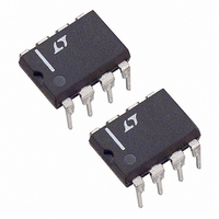
LTC1451CN8 Linear Technology, LTC1451CN8 Datasheet - Page 8

LTC1451CN8
Manufacturer Part Number
LTC1451CN8
Description
IC D/A CONV 12BIT R-R 8-DIP
Manufacturer
Linear Technology
Datasheet
1.LTC1452CN8PBF.pdf
(12 pages)
Specifications of LTC1451CN8
Settling Time
14µs
Number Of Bits
12
Data Interface
Serial
Number Of Converters
1
Voltage Supply Source
Single Supply
Power Dissipation (max)
2mW
Operating Temperature
0°C ~ 70°C
Mounting Type
Through Hole
Package / Case
8-DIP (0.300", 7.62mm)
Lead Free Status / RoHS Status
Contains lead / RoHS non-compliant
Available stocks
Company
Part Number
Manufacturer
Quantity
Price
Company:
Part Number:
LTC1451CN8
Manufacturer:
LT
Quantity:
5 510
Part Number:
LTC1451CN8#PBF
Manufacturer:
LINEAR/凌特
Quantity:
20 000
OPERATIO
LTC1451
LTC1452/LTC1453
Serial Interface
The data on the D
on the rising edge of the clock. The MSB is loaded first. The
DAC register loads the data from the shift register when
CS/LD is pulled high. The CLK is disabled internally when
CS/LD is high. Note: CLK must be low before CS/LD is
pulled low to avoid an extra internal clock pulse.
The buffered output of the 12-bit shift register is available
on the D
Multiple LTC1451/LTC1452/LTC1453s may be daisy-
chained together by connecting the D
pin of the next chip, while the CLK and CS/LD signals
remain common to all chips in the daisy chain. The serial
data is clocked to all of the chips, then the CS/LD signal is
pulled high to update all of them simultaneously.
8
OUT
pin which swings from GND to V
U
IN
input is loaded into the shift register
OUT
pin to the D
CC
.
IN
Reference
The LTC1451 includes an internal 2.048V reference, mak-
ing 1LSB equal to 1mV (gain of 2). The LTC1453 has an
internal reference of 1.22V with a full scale of 2.5V (gain of
2.05). The internal reference output is turned off when the
pin is forced above the reference voltage, allowing an
external reference to be connected to the reference pin.
The LTC1452 has no internal reference and the REF pin
must be driven externally. The buffer gain is 2, so the
external reference must be less than V
of driving the 8k minimum DAC resistor ladder.
Voltage Output
The LTC1451 family’s rail-to-rail buffered output can
source or sink 5mA over the entire operating temperature
range while pulling to within 300mV of the positive supply
voltage or ground. The output swings to within a few
millivolts of either supply rail when unloaded and has an
equivalent output resistance of 40 when driving a load to
the rails. The output can drive 1000pF without going into
oscillation.
CC
/2 and be capable
sn145123 145123fas


