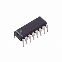
LTC7543KN Linear Technology, LTC7543KN Datasheet - Page 4

LTC7543KN
Manufacturer Part Number
LTC7543KN
Description
IC D/A CONV 12BIT SERIAL 16-DIP
Manufacturer
Linear Technology
Datasheet
1.LTC7543KN.pdf
(8 pages)
Specifications of LTC7543KN
Settling Time
250ns
Number Of Bits
12
Data Interface
Serial
Number Of Converters
1
Voltage Supply Source
Single Supply
Power Dissipation (max)
550µW
Operating Temperature
-40°C ~ 85°C
Mounting Type
Through Hole
Package / Case
16-DIP (0.300", 7.62mm)
Lead Free Status / RoHS Status
Contains lead / RoHS non-compliant
Available stocks
Company
Part Number
Manufacturer
Quantity
Price
Part Number:
LTC7543KN
Manufacturer:
LTNEAR
Quantity:
20 000
ELECTRICAL CHARACTERISTICS –
LTC7543/LTC8143
V
SYMBOL
Timing Characteristics (Note 3)
t
t
t
t
t
t
t
t
t
t
t
t
t
t
t
t
SRO Timing Characteristics (LTC8143 Only)
t
t
Power Supply
V
I
The
temperature range.
Note 1: 0.5LSB = 0.012% of full scale.
Note 2: Using internal feedback resistor.
Note 3: Guaranteed by design, not subject to test.
Note 4: I
register loaded with all 1s.
Note 5: Typical temperature coefficient is 100ppm/ C.
Note 6: OUT 1 load = 100 in parallel with 13pF.
Note 7: To 0.01% for a full-scale change, measured from falling edge of
LD1 or LD2.
4
DS1
DS2
DS3
DS4
DH1
DH2
DH3
DH4
SRI
STB1
STB3
STB1
STB3
LD1
ASB
CLR
PD
PD1
DD
DD
DD
, t
= 5V, V
, t
, t
, t
, t
LD2
denotes specifications which apply over the full operating
STB2
STB4
STB2
STB4
OUT1
, Strobe Pulse Width
, Strobe Pulse Width
REF
with DAC register loaded with all 0s or I
(t
(t
PARAMETER
Serial Input to Strobe Setup Time
Serial Input to Strobe Hold Time
Serial Input Data Pulse Width
Load Pulse Width
LSB Strobed into Input Register
to Load DAC Register Time
Clear Pulse Width
STB2, STB3, STB4 Strobe to SRO
Propagation Delay
STB1 to SRO Propagation Delay
Supply Voltage
Supply Current
STB
STB
= 10V, V
= 80ns)
= 80ns)
OUT1
= V
OUT2
= AGND = DGND = 0V, T
OUT2
CONDITIONS
STB1 Used as the Strobe
STB2 Used as the Strobe
STB3 Used as the Strobe
STB4 Used as the Strobe
STB1 Used as the Strobe
STB2 Used as the Strobe
STB3 Used as the Strobe
STB4 Used as the Strobe
(Note 11)
(Note 12)
C
C
Digital Inputs = 0V or V
Digital Inputs = V
with DAC
L
L
= 50pF
= 50pF
LTC7543/LTC8143
A
= T
IH
MIN
or V
to T
Note 8: V
from all 1s to all 0s.
Note 9: V
Note 10: Calculation from e
(J/K ); R = resistance ( ); T = resistor temperature ( K); B = bandwidth
(Hz).
Note 11: Minimum high time for STB1, STB2, STB4. Minimum low time
for STB3.
Note 12. Minimum low time for STB1, STB2, STB4. Minimum high time
for STB3.
DD
IL
MAX
, unless otherwise specified.
REF
REF
= 0V. DAC register contents changed from all 0s to all 1s or
= 6V
RMS
at 1kHz. DAC register loaded with all 1s.
n
= 4KTRB where: K = Boltzmann constant
MIN
4.75
140
220
150
50
20
30
50
80
80
80
80
80
80
0
0
0
LTC7543/LTC8143
ALL GRADES
TYP
– 30
– 30
120
– 5
10
25
55
55
80
5
5
MAX
5.25
0.1
2
UNITS
mA
mA
ns
ns
ns
ns
ns
ns
ns
ns
ns
ns
ns
ns
ns
ns
ns
ns
V


