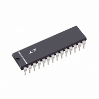
LTC1591-1CN#PBF Linear Technology, LTC1591-1CN#PBF Datasheet - Page 14

LTC1591-1CN#PBF
Manufacturer Part Number
LTC1591-1CN#PBF
Description
IC D/A CONV 14BIT PAR 28-DIP
Manufacturer
Linear Technology
Datasheet
1.LTC1591CGPBF.pdf
(20 pages)
Specifications of LTC1591-1CN#PBF
Settling Time
2µs
Number Of Bits
14
Data Interface
Parallel
Number Of Converters
1
Voltage Supply Source
Single Supply
Power Dissipation (max)
55µW
Operating Temperature
0°C ~ 70°C
Mounting Type
Through Hole
Package / Case
28-DIP (0.300", 7.62mm)
Lead Free Status / RoHS Status
Lead free / RoHS Compliant
LTC1591/LTC1597
APPLICATIONS
Bipolar Mode
(4-Quadrant Multiplying, V
The LTC1591/LTC1597 contain on chip all the 4-quadrant
resistors necessary for bipolar operation. 4-quadrant
multiplying operation can be achieved with a minimum of
external components, a capacitor and a dual op amp, as
shown in Figure 2. With a fixed 10V reference, the circuit
shown gives a precision bipolar – 10V to 10V output
swing.
Op Amp Selection
Because of the extremely high accuracy of the 14-/16-bit
LTC1591/LTC1597, thought should be given to op amp
selection in order to achieve the exceptional performance
of which the part is capable. Fortunately, the sensitivity of
INL and DNL to op amp offset has been greatly reduced
compared to previous generations of multiplying DACs.
Op amp offset will contribute mostly to output offset and
gain and will have minimal effect on INL and DNL. For the
LTC1597, a 500μV op amp offset will cause about 0.55LSB
INL degradation and 0.15LSB DNL degradation with a 10V
full-scale range. The main effects of op amp offset will be
a degradation of zero-scale error equal to the op amp
14
INPUTS
10 TO 21,
24 TO 27
DATA
CLR
WR
LD
16
V
REF
WR
9
3
R1
LD
8
R1
CLR
28
LTC1597
R
2
COM
R2
U
0.1μF
1
REF
INFORMATION
Figure 1b. Unipolar Operation (2-Quadrant Multiplication) V
U
OUT
5V
V
CC
23
= – V
R
4
R
OFS
OFS
W
16-BIT DAC
REF
R
FB
to V
R
5
FB
DGND
REF
U
I
OUT1
AGND
)
22
6
7
33pF
–
+
LT1001
offset, and a degradation of full-scale error equal to twice
the op amp offset. For the LTC1597, the same 500μV op
amp offset (2mV offset for LTC1591) will cause a 3.3LSB
zero-scale error and a 6.5LSB full-scale error with a 10V
full-scale range.
Op amp input bias current (I
scale error equal to I
thorough discussion of 16-bit DAC settling time and op
amp selection, refer to Application Note 74, “ Component
and Measurement Advances Ensure 16-Bit DAC Settling
Time .”
Reference Input and Grounding
For optimum performance the reference input of the
LTC1597 should be driven by a source impedance of less
than 1kΩ. However, these DACs have been designed to
minimize source impedance effects. An 8kΩ source im-
pedance degrades both INL and DNL by 0.2LSB.
As with any high resolution converter, clean grounding is
important. A low impedance analog ground plane and star
grounding should be used. AGND must be tied to the star
ground with as low a resistance as possible.
V
0V TO
–V
OUT
REF
=
OUT
1111
1000
0000
0000
MSB
= 0V to – V
IN DAC REGISTER
BINARY NUMBER
DIGITAL INPUT
BIAS
1111 1111 1111
0000 0000 0000
0000 0000 0001
0000 0000 0000
Unipolar Binary Code Table
(R
BIAS
REF
FB/
R
LSB
) contributes only a zero-
OFS
) = I
–V
–V
–V
0V
REF
REF
REF
ANALOG OUTPUT
(65,535/65,536)
(32,768/65,536) = –V
(1/65,536)
BIAS
V OUT
(6k). For a
1591/97 F01b
15917fa
REF
/2


