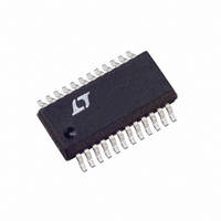
LTC1450LCG#PBF Linear Technology, LTC1450LCG#PBF Datasheet - Page 9

LTC1450LCG#PBF
Manufacturer Part Number
LTC1450LCG#PBF
Description
IC D/A CONV 12BIT R-R PAR 24SSOP
Manufacturer
Linear Technology
Datasheet
1.LTC1450CGPBF.pdf
(16 pages)
Specifications of LTC1450LCG#PBF
Settling Time
14µs
Number Of Bits
12
Data Interface
Parallel
Number Of Converters
1
Voltage Supply Source
Single Supply
Power Dissipation (max)
750µW
Operating Temperature
0°C ~ 70°C
Mounting Type
Surface Mount
Package / Case
24-SSOP
Lead Free Status / RoHS Status
Lead free / RoHS Compliant
Available stocks
Company
Part Number
Manufacturer
Quantity
Price
DEFI ITIO S
Resolution (n): Resolution is defined as the number of
digital input bits (n). It defines the number of DAC output
states (2
does not imply linearity.
Full-Scale Voltage (V
when all bits are set to 1.
Voltage Offset Error (V
output when the DAC is loaded with all zeros. The output
amplifier can have a true negative offset, but because the
part is operated from a single supply, the output cannot go
below zero. If the offset is negative, the output will remain
near 0V resulting in the transfer curve shown in Figure 1.
The offset of the part is measured at the code that corre-
sponds to the maximum offset specification:
Least Significant Bit (LSB): One LSB is the ideal voltage
difference between two successive codes.
Nominal LSBs:
V
LSB = (V
LTC1450
LTC1450L
OS
U
= V
n
) that divide the full-scale range. The resolution
OUT
FS
– V
– [(Code)(V
LSB = 4.095V/4095 = 1mV
LSB = 2.5V/4095 = 0.610mV
U
OS
)/(2
FS
OS
n
): This is the output of the DAC
): The theoretical voltage at the
– 1) = (V
FS
)/(2
n
– 1)]
FS
– V
NEGATIVE
OS
OFFSET
)/4095
VOLTAGE
Figure 1. Effect of Negative Offset
OUTPUT
0V
DAC CODE
Integral Nonlinearity (INL): End-point INL is the maxi-
mum deviation from a straight line passing through the
end points of the DAC transfer curve. Because the part
operates from a single supply and the output cannot go
below zero, the linearity is measured between full scale
and the code corresponding to the maximum offset
specification. The INL error at a given input code is
calculated as follows:
Differential Nonlinearity (DNL): DNL is the difference
between the measured change and the ideal one LSB
change between any two adjacent codes. The DNL error
between any two codes is calculated as follows:
Digital Feedthrough: The glitch that appears at the analog
output caused by AC coupling from the digital inputs when
they change state. The area of the glitch is specified in
(nV) s).
INL
V
DNL
OUT
V
OUT
= [V
= The output voltage of the DAC measured at
= ( V
= The measured voltage difference between
1450/50L • F01
the given input code
two adjacent codes
OUT
OUT
– V
– LSB)/LSB
LTC1450/LTC1450L
OS
– (V
FS
– V
OS
)(code/4095)]/LSB
9


