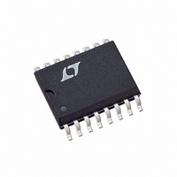
LTC1650CS Linear Technology, LTC1650CS Datasheet - Page 9

LTC1650CS
Manufacturer Part Number
LTC1650CS
Description
IC D/A CONV 16BIT R-R 16-SOIC
Manufacturer
Linear Technology
Datasheet
1.LTC1650ISPBF.pdf
(12 pages)
Specifications of LTC1650CS
Settling Time
4µs
Number Of Bits
16
Data Interface
Serial
Number Of Converters
1
Voltage Supply Source
Dual ±
Power Dissipation (max)
50mW
Operating Temperature
0°C ~ 70°C
Mounting Type
Surface Mount
Package / Case
16-SOIC (3.9mm Width)
Lead Free Status / RoHS Status
Contains lead / RoHS non-compliant
Available stocks
Company
Part Number
Manufacturer
Quantity
Price
Part Number:
LTC1650CS
Manufacturer:
LINEAR/凌特
Quantity:
20 000
Company:
Part Number:
LTC1650CS#PBF
Manufacturer:
Intersil
Quantity:
430
Part Number:
LTC1650CS#PBF
Manufacturer:
LINEAR/凌特
Quantity:
20 000
OPERATIO
Serial Interface
The data on the D
on the rising edge of the clock. Data is loaded as one
16-bit word, MSB first. The DAC register loads the data
from the shift register when CS/LD is pulled high. The
clock is disabled internally when CS/LD is high. Note: CLK
must be low before CS/LD is pulled low to avoid an extra
internal clock pulse.
The buffered output of the 16-bit shift register is available
on the D
Multiple LTC1650s may be daisy-chained together by
connecting the D
while the clock and CS/LD signals remain common to all
chips in the daisy chain. The serial data is clocked to all of
the chips, then the CS/LD signal is pulled high to update all
of them simultaneously.
When CLR is pulled low or when the part powers up, the
output connects through an internal pass gate to V
will go to whatever voltage is on V
supplies (DV
RSTOUT pin goes low and stays low as long as the supply
is below 2.5V. The power-on reset is also activated when
one of the supplies drops below 2.5V and the output is
then connected to V
when any of three conditions occur: CLR goes low, the part
powers up or one of the supplies drops below 2.5V. This
OUT
pin which swings from DGND to DV
DD
, AV
OUT
U
IN
input is loaded into the shift register
DD
RST
pin to the D
, |AV
. The output connects to V
SS
|) goes below 2.5V, the
RST
IN
pin of the next chip
. When any of three
DD
RST
.
and
RST
condition exists as long as CS/LD is low. As soon as CS/LD
goes high, the DAC register is loaded with the data in the
shift register and the output will settle to its new value.
Voltage Output
The LTC1650 rail-to-rail buffered output can source or
sink 5mA over the entire operating temperature range. The
output is specified to swing up to 4.5V on 4.75V
supplies with V
various load currents, refer to the typical curve “Minimum
Supply Headroom for Full Output Swing vs Load Cur-
rent.”) The buffer amplifier can drive 1000pF without
going into oscillation. The LTC1650 has a deglitched
voltage output. The midscale glitch is less than 2nV-s. The
digital feedthrough is about 0.05nV-s.
Output Ranges
The LTC1650 is capable of unipolar or bipolar output
swing. When the UNI/BIP pin is connected to V
is configured for unipolar operation and the output will
swing from REFLO to REFHI. When UNI/BIP is connected
to REFHI the part is configured in bipolar mode and the
output will swing from (2 • REFLO – REFHI) to REFHI and
will be at REFLO at midscale. With REFLO = 0V the output
swing is REFHI in bipolar mode and 0V to REFHI in
unipolar mode.
OUT
unloaded. (For typical output swing at
LTC1650
OUT
the part
9


