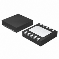
LTC2642CDD-16#PBF Linear Technology, LTC2642CDD-16#PBF Datasheet - Page 9

LTC2642CDD-16#PBF
Manufacturer Part Number
LTC2642CDD-16#PBF
Description
IC DAC 16BIT VOUT 10-DFN
Manufacturer
Linear Technology
Datasheet
1.LTC2642CDD-12PBF.pdf
(24 pages)
Specifications of LTC2642CDD-16#PBF
Settling Time
1µs
Number Of Bits
16
Data Interface
Serial
Number Of Converters
1
Voltage Supply Source
Single Supply
Power Dissipation (max)
600µW
Operating Temperature
0°C ~ 70°C
Mounting Type
Surface Mount
Package / Case
10-DFN
Number Of Channels
1
Resolution
16b
Interface Type
SER 3W SPI QSPI UW
Single Supply Voltage (typ)
3/5V
Dual Supply Voltage (typ)
Not RequiredV
Power Supply Requirement
Single
Output Type
Voltage
Integral Nonlinearity Error
±2LSB
Single Supply Voltage (min)
2.7V
Single Supply Voltage (max)
5.5V
Dual Supply Voltage (min)
Not RequiredV
Dual Supply Voltage (max)
Not RequiredV
Operating Temp Range
0C to 70C
Operating Temperature Classification
Commercial
Mounting
Surface Mount
Pin Count
10
Package Type
DFN EP
Lead Free Status / RoHS Status
Lead free / RoHS Compliant
Available stocks
Company
Part Number
Manufacturer
Quantity
Price
PIN FUNCTIONS
LTC2641 – MSOP, DFN Packages
REF (Pin 1): Reference Voltage Input. Apply an external
reference at REF between 2V and V
CS (Pin 2): Serial Interface Chip Select/Load Input. When
CS is low, SCLK is enabled for shifting in data on DIN.
When CS is taken high, SCLK is disabled, the 16-bit input
word is latched and the DAC is updated.
SCLK (Pin 3): Serial Interface Clock Input. CMOS and
TTL compatible.
DIN (Pin 4): Serial Interface Data Input. Data is applied
to DIN for transfer to the device at the rising edge of
SCLK.
CLR (Pin 5): Asynchronous Clear Input. A logic low clears
the DAC to code 0.
V
0V to V
V
5.5V.
GND (Pin 8): Circuit Ground.
Exposed Pad (DFN Pin 9): Circuit Ground. Must be sol-
dered to PCB ground.
LTC2641 – SO Package
V
0V to V
GND (Pin 2): Circuit Ground.
REF (Pin 3): Reference Voltage Input. Apply an external
reference at REF between 2V and V
CS (Pin 4): Serial Interface Chip Select/Load Input. When
CS is low, SCLK is enabled for shifting in data on DIN.
When CS is taken high, SCLK is disabled, the 16-bit input
word is latched and the DAC is updated.
SCLK (Pin 5): Serial Interface Clock Input. CMOS and
TTL compatible.
OUT
OUT
DD
(Pin 7): Supply Voltage. Set between 2.7V and
(Pin 6): DAC Output Voltage. The output range is
(Pin 1): DAC Output Voltage. The output range is
REF
REF
.
.
DD
DD
.
.
DIN (Pin 6): Serial Interface Data Input. Data is applied
to DIN for transfer to the device at the rising edge of
SCLK.
GND (Pin 7): Circuit Ground Pin. Must be connected to
Pin 2 (GND).
V
5.5V.
LTC2642 – MSOP , DFN Packages
REF (Pin 1): Reference Voltage Input. Apply an external
reference at REF between 2V and V
CS (Pin 2): Serial Interface Chip Select/Load Input. When
CS is low, SCLK is enabled for shifting in data on DIN.
When CS is taken high, SCLK is disabled, the 16-bit input
word is latched and the DAC is updated.
SCLK (Pin 3): Serial Interface Clock Input. CMOS and
TTL compatible.
DIN (Pin 4): Serial Interface Data Input. Data is applied
to DIN for transfer to the device at the rising edge of
SCLK.
CLR (Pin 5): Asynchronous Clear Input. A logic low clears
the DAC to midscale.
V
0V to V
INV (Pin 7): Center Tap of Internal Scaling Resistors. Con-
nect to an external amplifi er’s inverting input in bipolar
mode.
R
amplifi er’s output in bipolar mode. The bipolar output
range is –V
V
5.5V.
GND (Pin 10): Circuit Ground.
Exposed Pad (DFN Pin 11): Circuit Ground. Must be
soldered to PCB ground.
OUT
DD
DD
FB
(Pin 8): Feedback Resistor. Connect to an external
(Pin 8): Supply Voltage. Set between 2.7V and
(Pin 9): Supply Voltage. Set between 2.7V and
(Pin 6): DAC Output Voltage. The output range is
REF
.
REF
to V
REF
LTC2641/LTC2642
.
DD
.
26412fb
9


