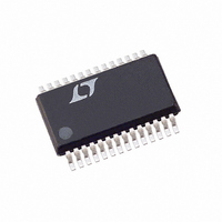
LTC1668IG Linear Technology, LTC1668IG Datasheet - Page 12

LTC1668IG
Manufacturer Part Number
LTC1668IG
Description
IC DAC 16BIT 50MSPS 28SSOP
Manufacturer
Linear Technology
Datasheet
1.LTC1668CGPBF.pdf
(24 pages)
Specifications of LTC1668IG
Settling Time
20ns
Number Of Bits
16
Data Interface
Parallel
Number Of Converters
1
Voltage Supply Source
Dual ±
Power Dissipation (max)
180mW
Operating Temperature
-40°C ~ 85°C
Mounting Type
Surface Mount
Package / Case
28-SSOP
Lead Free Status / RoHS Status
Contains lead / RoHS non-compliant
Available stocks
Company
Part Number
Manufacturer
Quantity
Price
Part Number:
LTC1668IG
Manufacturer:
LINEAR/凌特
Quantity:
20 000
Part Number:
LTC1668IG#PBF
Manufacturer:
ADI/亚德诺
Quantity:
20 000
Part Number:
LTC1668IG#PBF@@
Manufacturer:
LINEAR/凌特
Quantity:
20 000
Part Number:
LTC1668IG#TRPBF
Manufacturer:
LINEAR/凌特
Quantity:
20 000
LTC1666/LTC1667/LTC1668
APPLICATIO S I FOR ATIO
Adjusting the Full-Scale Output
In Figure 2, a serial interfaced DAC is used to set I
The LTC1661 is a dual 10-bit V
voltage output that swings from 0V to V
DAC Transfer Function
The LTC1666/LTC1667/LTC1668 use straight binary digital
coding. The complementary current outputs, I
B
nal), I
Code = 0) to 10mA when all bits are high (e.g., Code = 65535
for LTC1668) (decimal representation). I
mentary to I
formulas:
LTC1666:
LTC1667:
LTC1668:
In typical applications, the LTC1666/LTC1667/LTC1668
differential output currents either drive a resistive load
directly or drive an equivalent resistive load through a
transformer, or as the feedback resistor of an I-to-V
converter. The voltage outputs generated by the I
I
12
OUT B
, sink current from 0 to I
I
I
I
I
I
I
OUT A
OUT B
OUT A
OUT B
OUT A
OUT B
OUT A
output currents are then:
Figure 2. Adjusting the Full-Scale Current of
the LTC1666/LTC1667/LTC1668 with a DAC
= I
= I
= I
= I
= I
= I
5V
OUT A
swings from 0mA when all bits are low (e.g.,
OUTFS
OUTFS
OUTFS
OUTFS
OUTFS
OUTFS
1/2 LTC1661
. I
OUT A
• (DAC Code/4096)
• (4095 – DAC Code)/4096
• (DAC Code/16384)
• (16383 – DAC Code)/16384
• (DAC Code/65536)
• (65535 – DAC Code)/65536
REF
U
and I
OUTFS
U
0.1 F
OUT B
R
. For I
1.9k
SET
OUT
are given by the following
W
OUTFS
DAC with a buffered
I
REFIN
REFERENCE
REF
OUT B
+
–
2.5V
= 10mA (nomi-
.
OUT A
LTC1666/
LTC1667/
LTC1668
is comple-
U
1666/7/8
OUT A
and I
OUTFS
F03
and
OUT
(2)
(3)
(4)
(5)
(6)
(7)
.
The differential voltage is:
Substituting the values found earlier for I
I
From these equations some of the advantages of differen-
tial mode operation can be seen. First, any common mode
noise or error on I
signal power is twice as large as in the single-ended case.
Third, any errors and noise that multiply times I
I
midscale, where AC signal waveforms tend to spend the
most time. Fourth, this transfer function is bipolar; e.g. the
output swings positive and negative around a zero output
at mid-scale input, which is more convenient for AC
applications.
Note that the term (R
differential and single-ended transfer functions. This means
that the Gain Error of the DAC depends on the ratio of
R
temperature tracking of R
the absolute tempco of R
nonlinearity. As the DAC output changes from 0mA to
10mA the R
very low tempco can produce enough INL bowing to be
significant at the 16-bit level. This effect disappears with
medium to high frequency AC signals due to the slow
thermal time constant of the load resistor.
Analog Outputs
The LTC1666/LTC1667/LTC1668 have two complemen-
tary current outputs, I
Function). The output impedance of I
(R
Figure 3.)
OUTFS
OUT B
LOAD
IOUT A
V
V
V
V
(R
OUT A
OUT B
DIFF
DIFF
LOAD
, such as reference or I
to R
(LTC1668):
= V
= (I
= {2 • DAC Code – 65535)/65536} • 8 •
and R
/R
= I
= I
SET
OUT A
OUT A
LOAD
SET
OUT A
OUT B
, and the Gain Error tempco is affected by the
IOUT B
) • (V
resistor will heat up slightly, and even a
OUT A
– V
– I
• R
• R
) is typically 1.1k to LADCOM. (See
OUT B
REF
OUT B
LOAD
LOAD
OUT A
and I
LOAD
)
) • (R
LOAD
OUT B
LOAD
and I
/R
SET
LOAD
OUTFS
with R
is cancelled. Second, the
OUT B
is very critical for DC
) appears in both the
)
noise, cancel near
SET
(see DAC Transfer
OUT A
OUT A
. Note also that
, I
and I
OUT A
OUT B
OUT B
(10)
(11)
and
and
(8)
(9)


