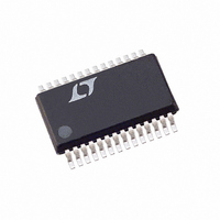
LTC1597ACG#TRPBF Linear Technology, LTC1597ACG#TRPBF Datasheet - Page 4

LTC1597ACG#TRPBF
Manufacturer Part Number
LTC1597ACG#TRPBF
Description
IC D/A CONV 16BIT PAR 28-SSOP
Manufacturer
Linear Technology
Datasheet
1.LTC1591CGPBF.pdf
(20 pages)
Specifications of LTC1597ACG#TRPBF
Settling Time
1µs
Number Of Bits
16
Data Interface
Parallel
Number Of Converters
1
Voltage Supply Source
Single Supply
Power Dissipation (max)
55µW
Operating Temperature
0°C ~ 70°C
Mounting Type
Surface Mount
Package / Case
28-SSOP
Lead Free Status / RoHS Status
Lead free / RoHS Compliant
Available stocks
Company
Part Number
Manufacturer
Quantity
Price
range. V
LTC1591/LTC1597
ELECTRICAL CHARACTERISTICS
SYMBOL
Analog Outputs (Note 4)
C
Digital Inputs
V
V
I
C
Timing Characteristics
t
t
t
t
t
t
Power Supply
V
I
Note 1: Stresses beyond those listed under Absolute Maximum Ratings
may cause permanent damage to the device. Exposure to any Absolute
Maximum Rating condition for extended periods may affect device
reliability and lifetime.
Note 2: ±1LSB = ±0.006% of full scale = ±61ppm of full scale for the
LTC1591/LTC1591-1. ±1LSB = ±0.0015% of full scale = ±15.3ppm of full
scale for the LTC1597/LTC1597-1.
Note 3: Using internal feedback resistor.
Note 4: Guaranteed by design, not subject to test.
Note 5: I
Note 6: Typical temperature coefficient is 100ppm/°C.
Note 7: I
Note 8: To 0.006% for a full-scale change, measured from the rising edge
of LD for the LTC1591/LTC1591-1. To 0.0015% for a full-scale change,
measured from the rising edge of LD for the LTC1597/LTC1597-1.
4
IN
DS
DH
WR
LD
CLR
LWD
DD
OUT
IH
IL
IN
DD
(OUT1)
OUT1
CC
= 5V ±10%, V
PARAMETER
Output Capacitance (Note 4)
Digital Input High Voltage
Digital Input Low Voltage
Digital Input Current
Digital Input Capacitance
Data to WR Setup Time
Data to WR Hold Time
WR Pulse Width
LD Pulse Width
Clear Pulse Width
WR to LD Delay Time
Supply Voltage
Supply Current
load = 100Ω in parallel with 13pF.
with DAC register loaded to all 0s.
REF
= 10V, I
OUT1
= AGND = DGND = 0V, T
CONDITIONS
DAC Register Loaded to All 1s: C
DAC Register Loaded to All 0s: C
(Note 4) V
Digital Inputs = 0V or V
IN
= 0V
The
●
denotes specifications that apply over the full operating temperature
A
= T
CC
Note 9: V
all 1s to all 0s.
Note 10: V
Note 11: Calculation from e
(J/°K), R = resistance (Ω), T = temperature (°K), B = bandwidth (Hz).
Note 12: Midscale transition code: 01 1111 1111 1111 to 10 0000 0000
0000 for the LTC1591/LTC1591-1 and 0111 1111 1111 1111 to 1000
0000 0000 0000 for the LTC1597/LTC1597-1.
Note 13: R1 and R2 are measured between R1 and R
Note 14: Measured using the LT1468 op amp in unipolar mode for I/V
converter and LT1468 I/V and LT1001 reference inverter in bipolar mode.
Sample Rate = 50kHz, Signal Frequency = 1kHz, V
MIN
to T
OUT1
OUT1
MAX
REF
REF
, unless otherwise noted.
= 0V. DAC register contents changed from all 0s to all 1s or
= 6V
RMS
at 1kHz. DAC register loaded with all 1s.
●
●
●
●
●
●
●
●
●
●
●
●
●
●
n
= √4kTRB where: k = Boltzmann constant
MIN
110
2.4
4.5
60
60
60
0
0
0.001
TYP
115
70
5
REF
COM
= 5V, T
MAX
130
0.8
5.5
±1
80
10
, REF and R
8
A
= 25°C.
UNITS
15917fa
COM
μA
μA
pF
pF
pF
ns
ns
ns
ns
ns
ns
.
V
V
V


