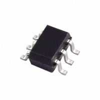
AD5621BKSZ-500RL7 Analog Devices Inc, AD5621BKSZ-500RL7 Datasheet - Page 9

AD5621BKSZ-500RL7
Manufacturer Part Number
AD5621BKSZ-500RL7
Description
IC DAC 12BIT SPI 5V SC70-6
Manufacturer
Analog Devices Inc
Series
nanoDAC™r
Datasheet
1.AD5601BKSZ-REEL7.pdf
(20 pages)
Specifications of AD5621BKSZ-500RL7
Data Interface
SPI™
Settling Time
6µs
Number Of Bits
12
Number Of Converters
1
Voltage Supply Source
Single Supply
Power Dissipation (max)
500µW
Operating Temperature
-40°C ~ 125°C
Mounting Type
Surface Mount
Package / Case
SC-70-6, SC-88, SOT-363
Resolution (bits)
12bit
Sampling Rate
1.7MSPS
Input Channel Type
Serial
Supply Voltage Range - Analog
2.7V To 5.5V
Supply Current
75µA
Digital Ic Case Style
SC-70
Number Of Channels
1
Resolution
12b
Interface Type
Serial (3-Wire, SPI, QSPI, Microwire)
Single Supply Voltage (typ)
3.3/5V
Dual Supply Voltage (typ)
Not RequiredV
Architecture
Resistor-String
Power Supply Requirement
Single
Output Type
Voltage
Integral Nonlinearity Error
±1LSB
Single Supply Voltage (min)
2.7V
Single Supply Voltage (max)
5.5V
Dual Supply Voltage (min)
Not RequiredV
Dual Supply Voltage (max)
Not RequiredV
Operating Temp Range
-40C to 125C
Operating Temperature Classification
Automotive
Mounting
Surface Mount
Pin Count
6
Package Type
SC-70
Lead Free Status / RoHS Status
Lead free / RoHS Compliant
Lead Free Status / RoHS Status
Lead free / RoHS Compliant, Lead free / RoHS Compliant
Available stocks
Company
Part Number
Manufacturer
Quantity
Price
Company:
Part Number:
AD5621BKSZ-500RL7
Manufacturer:
AD
Quantity:
11 650
CH1
CH2
CH1
CH2
2.458
2.456
2.454
2.452
2.450
2.448
2.446
2.444
2.442
2.440
2.438
2.436
0
V
T
A
DD
= 25°C
Figure 18. Digital-to-Analog Glitch Energy
= 5V
CH1 1V, CH2 20mV, TIME BASE = 20µs/DIV
Figure 16. Power-On Reset to 0 V
CH1 1V, CH2 5V, TIME BASE = 50µs/DIV
100
Figure 17. V
V
V
SAMPLE NUMBER
DD
OUT
200
DD
vs. V
V
DD
300
T
V
LOAD = 2kΩ AND 220pF
CODE 0x2000 TO 0x1FFF
10ns/SAMPLE NUMBER
OUT
V
A
DD
OUT
= 25°C
= 5V
= 70mV
V
T
400
DD
A
= 25°C
= 5V
500
Rev. E | Page 9 of 20
CH1
CH2
CH1
140
120
100
80
60
40
20
0
0
Figure 19. 1/f Noise, 0.1 Hz to 10 Hz Bandwidth
Figure 20. Exiting Power-Down Mode
CH1 5V, CH2 1V, TIME BASE = 2µs/DIV
5
Figure 21. I
FULL SCALE
AD5601/AD5611/AD5621
FREQUENCY (MHz)
10
CH1 5µV/DIV
DD
ZERO SCALE
vs. SCLK vs. Code
V
1/4 SCALE
OUT
15
V
T
MIDSCALE LOADED
DD
A
= 25°C
= 5V
V
T
A
MIDSCALE
DD
20
= 25°C
= 5V
3/4 SCALE
25


