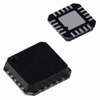
AD5424YCPZ-REEL7 Analog Devices Inc, AD5424YCPZ-REEL7 Datasheet - Page 19

AD5424YCPZ-REEL7
Manufacturer Part Number
AD5424YCPZ-REEL7
Description
IC DAC 8BIT MULTIPLYING 20-LFCSP
Manufacturer
Analog Devices Inc
Datasheet
1.AD5445YRUZ.pdf
(32 pages)
Specifications of AD5424YCPZ-REEL7
Settling Time
30ns
Number Of Bits
8
Data Interface
Parallel
Number Of Converters
1
Voltage Supply Source
Single Supply
Power Dissipation (max)
25µW
Operating Temperature
-40°C ~ 125°C
Mounting Type
Surface Mount
Package / Case
20-LFCSP
For Use With
EVAL-AD5424EBZ - BOARD EVALUATION FOR AD5424
Lead Free Status / RoHS Status
Lead free / RoHS Compliant
SINGLE-SUPPLY APPLICATIONS
Current Mode Operation
The current mode circuit in Figure 51 shows a typical circuit for
operation with a single 2.5 V to 5 V supply. I
I
configuration, the output voltage is given by
As D varies from 0 to 255 (AD5424), 0 to 1023 (AD5433),
or 0 to 4095 (AD5445), the output voltage varies from
V
sourcing all possible variations in current at the I
It is important to note that V
the switches in the DAC ladder no longer have the same source-
drain drive voltage. As a result, their on resistance differs and
the linearity of the DAC degrades.
Voltage Switching Mode of Operation
Figure 52 shows these DACs operating in the voltage-switching
mode. The reference voltage, V
I
at the V
voltage results in a positive output voltage, making single-
supply operation possible. The output from the DAC is voltage
at a constant impedance (the DAC ladder resistance), thus an
op amp is necessary to buffer the output voltage. The reference
input no longer sees a constant input impedance, but one that
varies with code. So, the voltage input should be driven from a
low impedance source.
OUT
OUT
V
BIAS
IN
1 is biased positive by the amount applied to V
2 is connected to AGND, and the output voltage is available
V
V
should be a low impedance source capable of sinking and
OUT
OUT
REF
NOTES:
1.
2.
= [D × (R
= V
ADDITIONAL PINS OMITTED FOR CLARITY
C1 PHASE COMPENSATION (1pF TO 2pF) MAY BE REQUIRED
IF A1 IS A HIGH SPEED AMPLIFIER.
terminal. In this configuration, a positive reference
Figure 51. Single-Supply Current Mode Operation
BIAS
V
REF
to V
FB
GND
V
V
/R
OUT
DD
DD
DAC
V
BIAS
DAC
= 2V
) × (V
IN
BIAS
R
is limited to low voltages because
IN
FB
I
I
OUT
OUT
BIAS
, is applied to the I
− V
1
2
– V
IN
.
IN
)] + V
C1
OUT
A1
BIAS
2 and therefore
OUT
BIAS
OUT
2 terminal.
. In this
1 pin,
V
OUT
Rev. B | Page 19 of 32
It is important to note that V
the switches in the DAC ladder no longer have the same source-
drain drive voltage. As a result, their on resistance differs, which
degrades the linearity of the DAC. See Figure 18 to Figure 23.
Also, V
an internal diode turns on, exceeding the maximum ratings of
the device. In this type of application, the full range of
multiplying capability of the DAC is lost.
POSITIVE OUTPUT VOLTAGE
Note that the output voltage polarity is opposite to the V
polarity for dc reference voltages. To achieve a positive voltage
output, an applied negative reference to the input of the DAC is
preferred over the output inversion through an inverting ampli-
fier because of the resistor tolerance errors. To generate a
negative reference, the reference can be level-shifted by an op
amp such that the V
the virtual ground and –2.5 V respectively, as shown
in Figure 53.
V
IN
+5V
–5V
Figure 53. Positive Voltage Output with Minimum of Components
V
Figure 52. Single-Supply Voltage-Switching Mode Operation
IN
OUT
ADR03
GND
NOTES:
1
2
must not go negative by more than 0.3 V,;otherwise,
ADDITIONAL PINS OMITTED FOR CLARITY.
C1 PHASE COMPENSATION (1pF TO 2pF) MAY BE REQUIRED,
IF A1 IS A HIGH SPEED AMPLIFIER.
NOTES:
–2.5V
1.
2.
I
I
OUT
OUT
V
ADDITIONAL PINS OMITTED FOR CLARITY
C1 PHASE COMPENSATION (1pF TO 2pF) MAY BE REQUIRED
IF A1 IS A HIGH SPEED AMPLIFIER.
IN
1
2
R
V
FB
REF
OUT
V
DAC
DD
V
V
GND
V
GND
DD
DD
and GND pins of the reference become
DD
= 5V
AD5424/AD5433/AD5445
IN
V
R
is limited to low voltages because
REF
FB
I
I
OUT
OUT
1
2
R1
C1
A1
R2
V
OUT
= 0V TO +2.5V
REF
V
OUT


