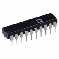
AD7945BNZ Analog Devices Inc, AD7945BNZ Datasheet - Page 3

AD7945BNZ
Manufacturer Part Number
AD7945BNZ
Description
IC DAC 12BIT MULT PARALL 20DIP
Manufacturer
Analog Devices Inc
Datasheet
1.AD7943BNZ.pdf
(16 pages)
Specifications of AD7945BNZ
Data Interface
Parallel
Settling Time
600ns
Number Of Bits
12
Number Of Converters
1
Voltage Supply Source
Single Supply
Power Dissipation (max)
25µW
Operating Temperature
-40°C ~ 85°C
Mounting Type
Through Hole
Package / Case
20-DIP (0.300", 7.62mm)
Resolution (bits)
12bit
Sampling Rate
1.7MSPS
Input Channel Type
Parallel
Supply Current
5µA
Digital Ic Case Style
DIP
No. Of Pins
20
Package
20PDIP N
Resolution
12 Bit
Conversion Rate
1.7 MSPS
Architecture
R-2R
Digital Interface Type
Parallel
Number Of Outputs Per Chip
1
Output Type
Current
Full Scale Error
±2 LSB
Integral Nonlinearity Error
±0.5 LSB
Maximum Settling Time
0.6(Typ) us
Lead Free Status / RoHS Status
Lead free / RoHS Compliant
Available stocks
Company
Part Number
Manufacturer
Quantity
Price
Part Number:
AD7945BNZ
Manufacturer:
ADI/亚德诺
Quantity:
20 000
SPECIFICATIONS
BIASED MODE
wise noted. AD7945, AD7948: V
Parameter
ACCURACY
DIGITAL INPUTS
DIGITAL OUTPUT (SRO)
POWER REQUIREMENTS
NOTES
1
2
3
Specifications subject to change without notice.
REV. B
These specifications apply with the devices biased up at 1.23 V for single supply applications. The model numbering reflects this by means of a “–B” suffix
Temperature ranges as follows: A Versions: –40 C to +85 C.
Guaranteed by design.
(for example: AD7943AN-B). Figure 16 is an example of Biased Mode Operation.
Resolution
Relative Accuracy
Differential Nonlinearity
Gain Error @ +25 C
Gain Temperature Coefficient
Output Leakage Current
Input Resistance
V
V
V
V
I
C
Output Low Voltage (V
Output High Voltage (V
V
Power Supply Sensitivity
I
I
INH
DD
DD
INH
INH
INL
INL
DD
IN
T
I
@ I
@ AGND Pin (AD7945, AD7948)
OUT1
, Input Capacitance
Gain/ V
MIN
, Input Current
(AD7943)
(AD7945, AD7948)
, Input Low Voltage @ V
, Input Low Voltage @ V
@ +25 C
T
, Input High Voltage @ V
, Input High Voltage @ V
Range
OUT2
MIN
to T
to T
Pin (AD7943)
DD
MAX
MAX
(AD7943: V
3
OL
OH
3
)
DD
)
= +3 V to +5.5 V; V
DD
DD
3
DD
DD
1
DD
= +5 V
= +3.3 V
= +3 V to +5.5 V; V
= +5 V
= +3.3 V
A Grades
12
2
5
10
100
6
6
2.4
2.1
0.8
0.6
10
0.2
V
3.0/5.5
–75
5
5
IOUT1
1
0.9
3
4
1
DD
– 0.2
= AGND = 1.23 V; V
IOUT1
= V
2
Units
Bits
LSB max
LSB max
LSB max
LSB max
ppm FSR/ C typ
ppm FSR/ C max
nA max
nA max
k min
k min
V min
V min
V max
V max
pF max
V max
V min
V min/V max
dB typ
IOUT2
A max
A max
A max
–3–
= AGND = 1.23 V; V
REF
= +0 V to 2.45 V; T
Test Conditions/Comments
1 LSB = (V
V
All Grades Guaranteed Monotonic
over Temperature
See Terminology Section
Typically 20 nA over Temperature
This Varies with DAC Input Code
For 1 CMOS Load
V
SRO Open Circuit; No STB Signal; Typically
1 A. Typically 100 A with 1 MHz STB
Frequency.
V
Typically 1 A.
IOUT1
INH
INH
REF
= +0 V to 2.45 V; T
= V
= V
AD7943/AD7945/AD7948
= 1.23 V and V
DD
DD
A
= T
IOUT1
– 0.1 V min, V
– 0.1 V min, V
MIN
to T
– V
MAX
REF)
A
REF
, unless otherwise noted.)
= T
/2
12
= 0 V
MIN
INL
INL
= 300 V When
to T
= 0.1 V max.
= 0.1 V max.
MAX
, unless other-


