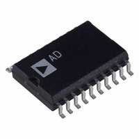
AD7305BRZ Analog Devices Inc, AD7305BRZ Datasheet - Page 6

AD7305BRZ
Manufacturer Part Number
AD7305BRZ
Description
IC DAC 8BIT QUAD 5V R-R 20-SOIC
Manufacturer
Analog Devices Inc
Datasheet
1.AD7304BRZ-REEL.pdf
(20 pages)
Specifications of AD7305BRZ
Data Interface
Parallel
Settling Time
1µs
Number Of Bits
8
Number Of Converters
4
Voltage Supply Source
Dual ±
Power Dissipation (max)
60mW
Operating Temperature
-40°C ~ 85°C
Mounting Type
Surface Mount
Package / Case
20-SOIC (7.5mm Width)
Resolution (bits)
8bit
Sampling Rate
1MSPS
Input Channel Type
Parallel
Supply Voltage Range - Analog
2.7V To 5.5V
Supply Current
6mA
Digital Ic Case Style
SOIC
Lead Free Status / RoHS Status
Lead free / RoHS Compliant
Available stocks
Company
Part Number
Manufacturer
Quantity
Price
Part Number:
AD7305BRZ
Manufacturer:
AD
Quantity:
20 000
Part Number:
AD7305BRZ-REEL
Manufacturer:
ADI/亚德诺
Quantity:
20 000
AD7304/AD7305
Table 4. AD7304 Control Logic Truth Table
CS
H
L
↑+
H
H
H
1
2
3
Table 5. AD7304 Serial Input Register Data Format, Data is Loaded in MSB-First Format
AD7304
If B11 (SAC), Shutdown All Channels, is set to logic low, all DACs are placed in a power shutdown mode, and all output voltages become
high resistance. If B10 (SDC), Shutdown Decoded Channel, is set to logic low, only the DAC decoded by Address Bits A1 and A0 is placed
in shutdown mode.
↑+ positive logic transition; ↓– negative logic transition; X Don’t Care.
One input register receives the data bits D7–D0 decoded from the SR address bits (A1, A0), where REG A = (0, 0), B = (0, 1), C = (1, 0), and D = (1, 1).
LDAC is a level-sensitive input.
1
CLK
X
↑+
L
X
X
X
1
MSB
B11
SAC
LDAC
H
H
H
L
H
H
B10
SDC
V
CLR
H
H
H
H
↓–
↑+
OUT
LDAC
LDAC
CLK
CLK
CLR
SDI
SDI
1
CS
FS
ZS
Serial Shift Register Function
No effect
Data advanced 1 bit
No effect
No effect
No effect
No effect
B9
A1
t
LD1
SDI/SHDN
SA
t
I
DD
CSS
SI
B8
A0
A1
t
CL
Figure 5. AD7304 Timing Diagram Zoom In
Figure 4. AD7304 General Timing Diagram
t
DS
A0
B7
D7
t
SDN
t
DH
D7
t
Rev. C | Page 6 of 20
CH
Input REG Function
No effect
No effect
Updated with SR contents
Latched with SR contents
Loaded with 0x00
Latched with 0x00
B6
D6
D6
D5
t
LDW
B5
D5
D4
t
S
D3
t
2
SDR
2
B4
D4
D2
ERROR BAND
DAC Register Function
No effect
No effect
No effect
All input register contents transferred
Loaded with 0x00
Latched with 0x00
±1 LSB
D1
t
CSH
B3
D3
D0
t
t
LD2
CLRW
t
S
B2
D2
B1
D1
3
LSB
B0
D0


