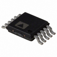
AD5663RBRMZ-3 Analog Devices Inc, AD5663RBRMZ-3 Datasheet

AD5663RBRMZ-3
Specifications of AD5663RBRMZ-3
Available stocks
Related parts for AD5663RBRMZ-3
AD5663RBRMZ-3 Summary of contents
Page 1
FEATURES Low power, smallest pin-compatible, dual nanoDAC AD5663R: 16 bits AD5643R: 14 bits AD5623R: 12 bits User-selectable external or internal reference External reference default On-chip 1.25 V/2 ppm/°C reference 10-lead MSOP and 3 mm × LFCSP ...
Page 2
AD5623R/AD5643R/AD5663R TABLE OF CONTENTS Features .............................................................................................. 1 Applications....................................................................................... 1 General Description ......................................................................... 1 Functional Block Diagram .............................................................. 1 Product Highlights ........................................................................... 1 Revision History ............................................................................... 2 Specifications..................................................................................... 3 AD5623R-5/AD5643R-5/AD5663R-5 ....................................... 3 AD5623R-3/AD5643R-3/AD5663R-3 ....................................... 5 AC Characteristics........................................................................ 6 Timing Characteristics ................................................................ ...
Page 3
SPECIFICATIONS AD5623R-5/AD5643R-5/AD5663R 4 5 kΩ to GND Table 2. Parameter 2 STATIC PERFORMANCE AD5663R Resolution Relative Accuracy Differential Nonlinearity AD5643R Resolution Relative Accuracy Differential Nonlinearity AD5623R Resolution Relative Accuracy ...
Page 4
AD5623R/AD5643R/AD5663R Parameter 3 LOGIC INPUTS Input Current Input Low Voltage (V ) INL Input High Voltage (V ) INH Pin Capacitance POWER REQUIREMENTS (Normal Mode 4 5 ...
Page 5
AD5623R-3/AD5643R-3/AD5663R 2 3 kΩ to GND Table 3. Parameter 2 STATIC PERFORMANCE AD5663R Resolution Relative Accuracy Differential Nonlinearity AD5643R Resolution Relative Accuracy Differential Nonlinearity AD5623R Resolution Relative Accuracy Differential ...
Page 6
AD5623R/AD5643R/AD5663R Parameter 3 LOGIC INPUTS Input Current V , Input Low Voltage INL V , Input High Voltage INH Pin Capacitance POWER REQUIREMENTS (Normal Mode 2 3 ...
Page 7
TIMING CHARACTERISTICS All input signals are specified with 2 5.5 V; all specifications T DD Table 5. Limit MIN MAX Parameter 5.5 V ...
Page 8
AD5623R/AD5643R/AD5663R ABSOLUTE MAXIMUM RATINGS T = 25°C, unless otherwise noted. A Table 6. Parameter V to GND GND OUT GND REFIN REFOUT Digital Input Voltage to GND Operating Temperature Range Industrial Storage Temperature Range ...
Page 9
PIN CONFIGURATION AND FUNCTION DESCRIPTIONS Table 7. Pin Function Descriptions Pin No. Mnemonic Description Analog Output Voltage from DAC A. The output amplifier has rail-to-rail operation. OUT Analog Output Voltage from DAC B. The ...
Page 10
AD5623R/AD5643R/AD5663R TYPICAL PERFORMANCE CHARACTERISTICS REF 25° –2 –4 –6 –8 – 10k 15k 20k 25k 30k 35k 40k 45k 50k 55k 60k 65k ...
Page 11
2.5V REFOUT T = 25° –2 –4 –6 –8 – 10k 15k 20k 25k 30k 35k 40k 45k 50k 55k 60k 65k CODE Figure 10. ...
Page 12
AD5623R/AD5643R/AD5663R 1.25V 8 REFOUT T = 25° –2 –4 –6 –8 – 10k 15k 20k 25k 30k 35k 40k 45k 50k 55k 60k 65k CODE Figure ...
Page 13
REF –2 –4 –6 –8 –40 – TEMPERATURE (°C) Figure 22. INL Error and DNL Error vs. Temperature ...
Page 14
AD5623R/AD5643R/AD5663R 1 25°C A 0.5 ZERO-SCALE ERROR 0 –0.5 –1.0 –1.5 –2.0 –2.5 2.7 3.2 3.7 4.2 V (V) DD Figure 28. Zero-Scale Error and Offset Error vs. Supply 25° ...
Page 15
T = 25° REFIN 0.25 0. REFIN 0.15 0.10 0.05 0 –40 – TEMPERATURE (°C) Figure 34. Supply Current vs. Temperature V ...
Page 16
AD5623R/AD5643R/AD5663R 2.496 2.494 2.492 2.490 2.488 2.486 2.484 2.482 2.480 2.478 2.476 2.474 2.472 2.470 2.468 2.466 2.464 V REFOUT 2.462 T = 25°C A 2.460 5ns/SAMPLE NUMBER 2.458 ANALOG CROSSTALK = 4.462nV 2.456 0 50 ...
Page 17
REF 25° CAPACITANCE (nF) Figure 46. Settling Time vs. Capacitive Load ...
Page 18
AD5623R/AD5643R/AD5663R TERMINOLOGY Relative Accuracy or Integral Nonlinearity (INL) For the DAC, relative accuracy or integral nonlinearity is a measurement of the maximum deviation, in LSBs, from a straight line passing through the endpoints of the DAC transfer function. A typical ...
Page 19
Digital Crosstalk Digital crosstalk is the glitch impulse transferred to the output of one DAC at midscale in response to a full-scale code change (all 0s to all 1s and vice versa) in the input register of another DAC. It ...
Page 20
AD5623R/AD5643R/AD5663R THEORY OF OPERATION DIGITAL-TO-ANALOG SECTION The AD5623R/AD5643R/AD5663R DAC is fabricated on a CMOS process. The architecture consists of a string DAC followed by an output buffer amplifier. Figure 49 shows a block diagram of the DAC architecture ...
Page 21
At this stage, the SYNC line can be kept low or be brought high. In either case, it must be brought high for a minimum before the next write sequence, so that a falling edge of SYNC ...
Page 22
AD5623R/AD5643R/AD5663R POWER-ON RESET The AD5623R/AD5643R/AD5663R contain a power-on reset circuit that controls the output voltage during power-up. The AD5623R/AD5643R/AD5663R DACs output power and the output remains there until a valid write sequence is made to the ...
Page 23
Table 13. 24-Bit Input Shift Register Contents of Power Up/Down Function MSB DB23 to DB22 DB21 DB20 DB19 DB18 Don’t Command bits (C2 to C0) Address bits (A2 to A0) care Don’t care Table 14. ...
Page 24
AD5623R/AD5643R/AD5663R INTERNAL REFERENCE SETUP The on-chip reference is off at power-up by default. This reference can be turned on or off by setting a software programmable bit, DB0, in the control register. Table 16 shows how the state of the ...
Page 25
MICROPROCESSOR INTERFACING AD5623R/AD5643R/AD5663R to Blackfin® ADSP-BF53X Interface Figure 56 shows a serial interface between the AD5623R/ AD5643R/AD5663R and the Blackfin ADSP-BF53X processor. The ADSP-BF53X processor family incorporates two dual-channel synchronous serial ports, SPORT1 and SPORT0, for serial and multiprocessor communications. ...
Page 26
AD5623R/AD5643R/AD5663R APPLICATIONS INFORMATION USING A REFERENCE AS A POWER SUPPLY Because the supply current required by the AD5623R/AD5643R/ AD5663R is extremely low, an alternative option is to use a voltage reference to supply the required voltage to the parts (see ...
Page 27
The power supply to the AD5663R should be bypassed with 10 μF and 0.1 μF capacitors. The capacitors should be located as close as possible to the device, with the 0.1 μF capacitor ideally right up against the device. The ...
Page 28
... AD5643RBRMZ-5REEL7 −40°C to +105°C AD5663RBCPZ-3R2 −40°C to +105°C AD5663RBCPZ-3REEL7 −40°C to +105°C AD5663RBRMZ-3 −40°C to +105°C AD5663RBRMZ-3REEL7 −40°C to +105°C AD5663RBRMZ-5 −40°C to +105°C AD5663RBRMZ-5REEL7 −40°C to +105°C EVAL-AD5663REBZ RoHS Compliant Part. ...


