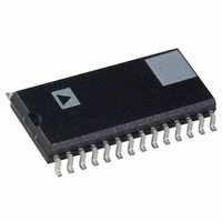
AD9760AR Analog Devices Inc, AD9760AR Datasheet - Page 2

AD9760AR
Manufacturer Part Number
AD9760AR
Description
IC DAC 10BIT 125MSPS 28-SOIC
Manufacturer
Analog Devices Inc
Series
TxDAC®r
Datasheet
1.AD9760ARUZ.pdf
(23 pages)
Specifications of AD9760AR
Mounting Type
Surface Mount
Rohs Status
RoHS non-compliant
Settling Time
35ns
Number Of Bits
10
Number Of Converters
1
Voltage Supply Source
Analog and Digital
Power Dissipation (max)
175mW
Operating Temperature
-40°C ~ 85°C
Package / Case
28-SOIC (7.5mm Width)
Update Rate
125MSPS
Peak Reflow Compatible (260 C)
No
Supply Voltage
5V
No. Of Bits
10 Bit
Leaded Process Compatible
No
Interface Type
Parallel
Resolution
10-Bit
For Use With
AD9760-EBZ - BOARD EVAL FOR AD9760
Data Interface
-
Lead Free Status / RoHS Status
Contains lead / RoHS non-compliant
Available stocks
Company
Part Number
Manufacturer
Quantity
Price
Part Number:
AD9760AR
Manufacturer:
ADI/亚德诺
Quantity:
20 000
Part Number:
AD9760AR50
Manufacturer:
ADI/亚德诺
Quantity:
20 000
Part Number:
AD9760ARU
Manufacturer:
ADI/亚德诺
Quantity:
20 000
Part Number:
AD9760ARU50
Manufacturer:
ADI/亚德诺
Quantity:
20 000
Part Number:
AD9760ARUZ
Manufacturer:
ADI/亚德诺
Quantity:
20 000
Company:
Part Number:
AD9760ARZ-REEL
Manufacturer:
AD
Quantity:
3 400
DC SPECIFICATIONS
Parameter
RESOLUTION
DC ACCURACY
MONOTONICITY
ANALOG OUTPUT
REFERENCE OUTPUT
REFERENCE INPUT
TEMPERATURE COEFFICIENTS
POWER SUPPLY
OPERATING RANGE
NOTES
1
2
3
4
5
6
7
Specifications subject to change without notice.
AD9760/AD9760-50–SPECIFICATIONS
Measured at I
Nominal full-scale current, I
Use an external buffer amplifier to drive any external load.
Reference bandwidth is a function of external cap at COMP1 pin and signal level. Refer to Figure 41.
For operation below 3 V, it is recommended that the output current be reduced to 12 mA or less to maintain optimum performance.
Measured at f
Measured as unbuffered voltage output into 50 Ω R
Integral Linearity Error (INL)
Differential Nonlinearity (DNL)
Offset Error
Gain Error (Without Internal Reference)
Gain Error (With Internal Reference)
Full-Scale Output Current
Output Compliance Range
Output Resistance
Output Capacitance
Reference Voltage
Reference Output Current
Input Compliance Range
Reference Input Resistance
Small Signal Bandwidth (w/o C
Offset Drift
Gain Drift (Without Internal Reference)
Gain Drift (With Internal Reference)
Reference Voltage Drift
Supply Voltages
Analog Supply Current (I
Digital Supply Current (I
Supply Current Sleep Mode (I
Power Dissipation
Power Dissipation
Power Dissipation
Power Supply Rejection Ratio—AVDD
Power Supply Rejection Ratio—DVDD
AVDD
DVDD
5
CLOCK
OUTA
, driving a virtual ground.
= 50 MSPS and f
1
6
7
7
(5 V, I
(5 V, I
(3 V, I
OUTFS
DVDD
, is 32 × the I
AVDD
OUTFS
OUTFS
OUTFS
3
2
OUT
(T
)
)
AVDD
MIN
6
COMP1
= 1.0 MHz.
= 20 mA)
= 20 mA)
= 2 mA)
to T
)
REF
)
MAX
4
current.
LOAD
, AVDD = +5 V, DVDD = +5 V, I
at I
OUTA
and I
OUTB
Min
10
–1.0
–0.5
Guaranteed Over Specified Temperature Range
–0.025
–10
–10
2.0
–1.0
1.08
0.1
2.7
2.7
–0.04
–40
–0.025
, f
CLOCK
–2–
= 100 MSPS and f
OUTFS
= 20 mA, unless otherwise noted)
Typ
± 0.5
± 0.25
± 2
± 1
100
5
1.20
100
1
1.4
0
± 50
± 100
± 50
5.0
5.0
25
3
140
190
45
OUT
= 40 MHz.
Max
+1.0
+0.5
+0.025
+10
+10
20.0
1.25
1.32
1.25
5.5
5.5
30
5
8.5
175
+0.04
+0.025
+85
Units
Bits
LSB
LSB
% of FSR
% of FSR
% of FSR
mA
V
kΩ
pF
V
nA
V
MΩ
MHz
ppm of FSR/°C
ppm of FSR/°C
ppm of FSR/°C
ppm/°C
V
V
mA
mA
mA
mW
mW
mW
% of FSR/V
% of FSR/V
°C
REV. B


