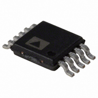
AD5322BRMZ Analog Devices Inc, AD5322BRMZ Datasheet - Page 4

AD5322BRMZ
Manufacturer Part Number
AD5322BRMZ
Description
IC DAC 12BIT DUAL 10MSOP
Manufacturer
Analog Devices Inc
Datasheet
1.AD5302ARMZ.pdf
(24 pages)
Specifications of AD5322BRMZ
Data Interface
Serial
Settling Time
6µs
Number Of Bits
12
Number Of Converters
2
Voltage Supply Source
Single Supply
Power Dissipation (max)
2.5mW
Operating Temperature
-40°C ~ 105°C
Mounting Type
Surface Mount
Package / Case
10-MSOP, Micro10™, 10-uMAX, 10-uSOP
Resolution (bits)
12bit
Sampling Rate
125kSPS
Input Channel Type
Serial
Supply Voltage Range - Analog
2.5V To 5.5V
Supply Current
300µA
Digital Ic Case Style
SOP
Package
10MSOP
Resolution
12 Bit
Conversion Rate
125 KSPS
Architecture
Resistor-String
Digital Interface Type
Serial (3-Wire, SPI, QSPI, Microwire)
Number Of Outputs Per Chip
2
Output Type
Voltage
Full Scale Error
±1 %FSR
Integral Nonlinearity Error
±8 LSB
Maximum Settling Time
10 us
Lead Free Status / RoHS Status
Lead free / RoHS Compliant
Available stocks
Company
Part Number
Manufacturer
Quantity
Price
Part Number:
AD5322BRMZ
Manufacturer:
ADI/亚德诺
Quantity:
20 000
Part Number:
AD5322BRMZ-REEL7
Manufacturer:
ADI/亚德诺
Quantity:
20 000
AD5302/AD5312/AD5322
Parameter
POWER REQUIREMENTS
1
2
3
4
5
6
AC SPECIFICATIONS
V
Table 2.
Parameter
Output Voltage Settling Time
Slew Rate
Major-Code Transition Glitch Energy
Digital Feedthrough
Analog Crosstalk
DAC-to-DAC Crosstalk
Multiplying Bandwidth
Total Harmonic Distortion
1
2
3
Temperature range: A, B version: –40°C to +105°C.
See Terminology section.
DC specifications tested with the outputs unloaded.
Linearity is tested using a reduced code range: AD5302 (Code 8 to 248); AD5312 (Code 28 to 995); AD5322 (Code 115 to 3981).
Guaranteed by design and characterization, not production tested.
In order for the amplifier output to reach its minimum voltage, offset error must be negative. In order for the amplifier output to reach its maximum voltage,
V
Guaranteed by design and characterization, not production tested.
Temperature range: A, B version: −40°C to +105°C.
See Terminology section.
DD
V
I
I
REF
DD
DD
AD5302
AD5312
AD5322
DD
V
V
V
V
= V
= 2.5 V to 5.5 V, R
(Normal Mode)
(Full Power-Down)
DD
DD
DD
DD
DD
= 4.5 V to 5.5 V
= 2.5 V to 3.6 V
= 4.5 V to 5.5 V
= 2.5 V to 3.6 V
and offset plus gain error must be positive.
2
3
L
= 2 kΩ to GND, C
Min
2.5
A Version
Typ
300
230
0.2
0.05
L
Min
= 200 pF to GND, all specifications T
1
Max
5.5
450
350
1
1
A, B Version
Typ
6
7
8
0.7
12
0.10
0.01
0.01
200
−70
Min
2.5
Max
8
9
10
2
B Version
Rev. C | Page 4 of 24
Typ
300
230
0.2
0.05
Unit
μs
μs
μs
nV-s
nV-s
nV-s
nV-s
kHz
dB
V/μs
1
Max
5.5
450
350
1
1
¼ Scale to ¾ Scale Change (0 × 40 to 0 × C0)
¼ Scale to ¾ Scale Change (0 × 100 to 0 × C300)
¼ Scale to ¾ Scale Change (0 × 400 to 0 × C00)
V
V
Test Conditions/Comments
V
1 LSB Change Around Major Carry (011…11 to 100…00)
REF
REF
REF
= V
= 2 V ± 0.1 V p-p, Unbuffered Mode
= 2.5 V ± 0.1 V p-p, Frequency = 10 kHz
μA
Unit
V
μA
μA
μA
MIN
DD
to T
= 5 V
MAX
Both DACs in unbuffered mode, V
, unless otherwise noted.
Test Conditions/Comments
I
Both DACs active and excluding load currents
V
typically × μA per DAC where x = 5 μA + V
DD
IL
specification is valid for all DAC codes
= GND; in buffered mode, extra current is
1
IH
= V
DD
and
REF
/R
DAC


