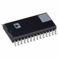
AD9744AR Analog Devices Inc, AD9744AR Datasheet - Page 5

AD9744AR
Manufacturer Part Number
AD9744AR
Description
IC DAC 14BIT 210MSPS 28-SOIC
Manufacturer
Analog Devices Inc
Series
TxDAC®r
Datasheet
1.AD9744ARUZ.pdf
(32 pages)
Specifications of AD9744AR
Rohs Status
RoHS non-compliant
Settling Time
11ns
Number Of Bits
14
Data Interface
Parallel
Number Of Converters
1
Voltage Supply Source
Analog and Digital
Power Dissipation (max)
145mW
Operating Temperature
-40°C ~ 85°C
Mounting Type
Surface Mount
Package / Case
28-SOIC (7.5mm Width)
Number Of Channels
1
Resolution
14b
Interface Type
Parallel
Single Supply Voltage (typ)
3.3V
Dual Supply Voltage (typ)
Not RequiredV
Power Supply Requirement
Analog and Digital
Output Type
Current
Integral Nonlinearity Error
±5LSB
Single Supply Voltage (min)
2.7V
Single Supply Voltage (max)
3.6V
Dual Supply Voltage (min)
Not RequiredV
Dual Supply Voltage (max)
Not RequiredV
Operating Temp Range
-40C to 85C
Operating Temperature Classification
Industrial
Mounting
Surface Mount
Pin Count
28
Package Type
SOIC W
For Use With
AD9744ACP-PCBZ - BOARD EVAL FOR AD9744ACP
Lead Free Status / Rohs Status
Not Compliant
Available stocks
Company
Part Number
Manufacturer
Quantity
Price
Part Number:
AD9744AR
Manufacturer:
ADI/亚德诺
Quantity:
20 000
Part Number:
AD9744ARU
Manufacturer:
ADI/亚德诺
Quantity:
20 000
Part Number:
AD9744ARUZ
Manufacturer:
ADI/亚德诺
Quantity:
20 000
Part Number:
AD9744ARZ
Manufacturer:
ADI/亚德诺
Quantity:
20 000
Parameter
1
2
3
DIGITAL SPECIFICATIONS
T
Table 3.
Parameter
DIGITAL INPUTS
CLK INPUTS
1
2
Measured single-ended into 50 Ω load.
Output noise is measured with a full-scale output set to 20 mA with no conversion activity. It is a measure of the thermal noise only.
Noise spectral density is the average noise power normalized to a 1 Hz bandwidth, with the DAC converting and producing an output tone.
Includes CLOCK pin on SOIC/TSSOP packages and CLK+ pin on LFCSP package in single-ended clock input mode.
Applicable to CLK+ and CLK– inputs when configured for differential or PECL clock input mode.
MIN
Multitone Power Ratio (8 Tones at 400 kHz Spacing)
Logic 1 Voltage
Logic 0 Voltage
Logic 1 Current
Logic 0 Current
Input Capacitance
Input Setup Time (t
Input Hold Time (t
Latch Pulse Width (t
Input Voltage Range
Common-Mode Voltage
Differential Voltage
f
to T
CLOCK
0 dBFS Output
−6 dBFS Output
−12 dBFS Output
−18 dBFS Output
MAX
= 78 MSPS; f
2
, AVDD = 3.3 V, DVDD = 3.3 V, CLKVDD = 3.3 V, I
1
H
S
)
OUT
)
LPW
)
= 15.0 MHz to 18.2 MHz
DB0–DB13
CLOCK
IOUTA
IOUTB
OR
t
S
Figure 2. Timing Diagram
Rev. B | Page 5 of 32
t
PD
OUTFS
0.1%
= 20 mA, unless otherwise noted.
Min
2.1
−10
−10
2.0
1.5
1.5
0
0.75
0.5
t
t
ST
LPW
t
H
0.1%
Min
Typ
3
0
5
1.5
1.5
Typ
66
68
62
61
Max
0.9
+10
+10
3
2.25
Max
Unit
V
V
µA
µA
pF
ns
ns
ns
V
V
V
Unit
dBc
dBc
dBc
dBc
AD9744


