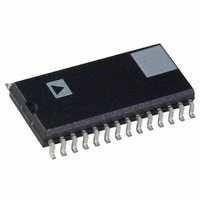
DAC8408FSZ Analog Devices Inc, DAC8408FSZ Datasheet - Page 11

DAC8408FSZ
Manufacturer Part Number
DAC8408FSZ
Description
IC DAC 8BIT QUAD W/MEMORY 28SOIC
Manufacturer
Analog Devices Inc
Datasheet
1.DAC8408FSZ-REEL.pdf
(16 pages)
Specifications of DAC8408FSZ
Data Interface
Parallel
Settling Time
190ns
Number Of Bits
8
Number Of Converters
4
Voltage Supply Source
Single Supply
Operating Temperature
-40°C ~ 85°C
Mounting Type
Surface Mount
Package / Case
28-SOIC (7.5mm Width)
Resolution (bits)
8bit
Input Channel Type
Parallel
Supply Voltage Range - Analogue
4.5V To 5.5V
Supply Current
50µA
Digital Ic Case Style
SOIC
No. Of
RoHS Compliant
Number Of Channels
4
Resolution
8b
Interface Type
Parallel
Single Supply Voltage (typ)
5V
Dual Supply Voltage (typ)
Not RequiredV
Architecture
R-2R
Power Supply Requirement
Single
Output Type
Current
Single Supply Voltage (min)
4.5V
Single Supply Voltage (max)
5.5V
Dual Supply Voltage (min)
Not RequiredV
Dual Supply Voltage (max)
Not RequiredV
Operating Temp Range
-40C to 85C
Operating Temperature Classification
Industrial
Mounting
Surface Mount
Pin Count
28
Lead Free Status / RoHS Status
Lead free / RoHS Compliant
Power Dissipation (max)
-
Lead Free Status / Rohs Status
Compliant
Available stocks
Company
Part Number
Manufacturer
Quantity
Price
Part Number:
DAC8408FSZ
Manufacturer:
ADI/亚德诺
Quantity:
20 000
REV. A
DAC Data Input
MSB
1 1 1 1 1 1 1 1
1 0 0 0 0 0 0 1
1 0 0 0 0 0 0 0
0 1 1 1 1 1 1 1
0 0 0 0 0 0 0 1
0 0 0 0 0 0 0 0
NOTE
1 LSB = (2
Table II. Bipolar (Offset Binary) Code Table
(Refer to Figure 7)
–7
) (V
REF
LSB
) =
128
1
(V
REF
)
Figure 7. Quad DAC Bipolar Operation (4-Quadrant Multiplication)
Analog Output
(DAC A OR DAC B)
+V
+V
0
–V
–V
–V
REF
REF
REF
REF
REF
128
127
128
128
128
127
128
128
1
1
–11–
APPLICATION HINTS
General Ground Management: AC or transient voltages be-
tween AGND and DGND can appear as noise at the DAC8408’s
analog output. Note that in Figures 5 and 6, I
I
ommended that AGND and DGND be tied together at the
DAC8408 socket. In systems where AGND and DGND are tied
together on the backplane, two diodes (1N914 or equivalent)
should be connected in inverse parallel between AGND and
DGND.
Write Enable Timing: During the period when both DS and
R/W are held low, the DAC latches are transparent and the ana-
log output responds directly to the digital data input. To pre-
vent unwanted variations of the analog output, the R/W should
not go low until the data bus is fully settled (DATA VALID).
OUT 2C
/I
OUT 2D
are connected to AGND. Therefore, it is rec-
DAC8408
OUT2A
/I
OUT2B
and


