AD667JP Analog Devices Inc, AD667JP Datasheet - Page 2
AD667JP
Manufacturer Part Number
AD667JP
Description
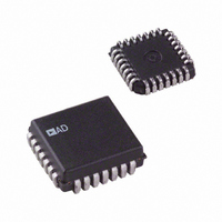
IC DAC 12BIT V-OUT 28-PLCC
Manufacturer
Analog Devices Inc
Datasheet
1.AD667JNZ.pdf
(8 pages)
Specifications of AD667JP
Rohs Status
RoHS non-compliant
Settling Time
3µs
Number Of Bits
12
Number Of Converters
1
Voltage Supply Source
Dual ±
Power Dissipation (max)
1W
Operating Temperature
0°C ~ 70°C
Mounting Type
Surface Mount
Package / Case
28-LCC (J-Lead)
Data Interface
-
Available stocks
Company
Part Number
Manufacturer
Quantity
Price

Part Number:
AD667JP
Manufacturer:
ADI/亚德诺
Quantity:
20 000
Part Number:
AD667JPZ
Manufacturer:
ADI/亚德诺
Quantity:
20 000
Company:
Part Number:
AD667JPZ-REEL
Manufacturer:
Analog Devices Inc
Quantity:
10 000


AD667–SPECIFICATIONS
TIMING SPECIFICATIONS
(All Models, T
Symbol
t
t
t
t
t
Model
DIGITAL INPUTS
TRANSFER CHARACTERISTICS
DRIFT
CONVERSION SPEED
ANALOG OUTPUT
REFERENCE OUTPUT
POWER SUPPLY SENSITIVITY
POWER SUPPLY REQUIREMENTS
TEMPERATURE RANGE
NOTES
1
2
3
4
Specifications subject to change without notice.
Specifications shown in boldface are tested on all production units at final electrical
test. Results from those tests are used to calculate outgoing quality levels. All min and
max specifications are guaranteed, although only those shown in boldface are tested
on all production units.
DC
AC
CP
DH
SETT
The digital input specifications are 100% tested at +25 C, and guaranteed but not tested over the full temperature range.
Adjustable to zero.
FSR means “Full-Scale Range” and is 20 V for 10 V range and 10 V for the 5 V range.
A minimum power supply of 12.5 V is required for a 10 V full-scale output and 11.4 V is required for all other voltage ranges.
Resolution
Logic Levels (TTL, Compatible, T
V
V
I
I
ACCURACY
Differential Linearity Error @ +25 C
Gain Error
Unipolar Offset Error
Bipolar Zero
Differential Linearity
Gain (Full Scale) T
Unipolar Offset T
Bipolar Zero T
Settling Time to 0.01% of FSR for
Slew Rate
Ranges
Output Current
Output Impedance (DC)
Short Circuit Current
External Current
V
V
Rated Voltages
Range
Supply Current
Specification
Storage
IH
IL
IH
IL
CC
EE
T
Linearity Error @ +25 C
FSR Change (2 k
For LSB Change
+11.4 V to +16.5 V dc
–11.4 V to –16.5 V dc
(V
(V
(Logic “0”)
A
(Logic “l’’)
= –11.4 V to –16.5 V dc
= +11.4 V to +16.5 V dc
T
with 10 k Feedback
with 5 k Feedback
IL
= T
IH
4
A
4
= 0.8 V)
= 5.5 V)
= T
Parameter
Data Valid to End of CS
Address Valid to End of CS
CS Pulse Width
Data Hold Time
Output Voltage Settling Time
MIN
2
A
MIN
2
to T
= +25 C, V
A
to T
= 25 C to T
A
MAX
A
= –25 C to T
MAX
= 25 C to T
2
500 pF Load)
CC
= +12 V or +15 V, V
MIN
MIN
MIN
or T
MIN
or T
or T
MAX
–T
MAX
MAX
MAX
)
1
Min
50
100
100
0
–
EE
Min
+2.0
0
10
9.90
0.1
0
–65
= –12 V or –15 V)
5
11.4
Typ
–
_
–
–
2
Monotonicity Guaranteed
(@ T
Max
–
_
–
–
4
AD667J
Typ
3
1
+1/4
3
2
1
+5, +10
0.05
10.00
1.0
5
5
8
20
1/2
1/2
0.1
1
0.05
2
5
1
5
2.5, 5, 10,
12, 15
A
= +25 C,
ns
ns
ns
ns
s
–2–
12 V,
ABSOLUTE MAXIMUM RATINGS
V
V
Digital Inputs (Pins 11–15, 17–28)
Ref In to Reference Ground . . . . . . . . . . . . . . . . . . . . . .
Bipolar Offset to Reference Ground . . . . . . . . . . . . . . . .
10 V Span R to Reference Ground . . . . . . . . . . . . . . . . .
20 V Span R to Reference Ground . . . . . . . . . . . . . . . . .
Ref Out, V
Power Dissipation . . . . . . . . . . . . . . . . . . . . . . . . . . 1000 mW
CC
EE
Max
12
+5.5
+0.8
10
5
4
3
10.10
10
10
12
25
+70
+125
40
to Power Ground . . . . . . . . . . . . . . . . . . . . –1.0 V to +7.0 V
30
3
10
1/2
3/4
3/4
0.2
2
0.1
16.5
. . . . . . . . . . . . . . . . . . . . . . . . . . . Momentary Short to V
to Power Ground . . . . . . . . . . . . . . . . . . . . . 0 V to –18 V
to Power Ground . . . . . . . . . . . . . . . . . . . . . 0 V to +18 V
15 V power supplies unless otherwise noted)
OUT
Min
+2.0
0
10
9.90
0.1
0
–65
5
11.4
(Pins 6, 9) . . Indefinite Short to Power Ground
Monotonicity Guaranteed
AD667K
Typ
3
1
3
2
1
+5, +10
0.05
10.00
1.0
5
5
8
20
1/8
1/4
1/4
0.1
1
0.05
2
5
2.5, 5, 10,
12, 15
Max
12
+5.5
+0.8
10
5
4
3
40
10.10
10
10
12
25
+70
+125
15
3
10
1/4
1/2
1/2
0.2
2
0.1
16.5
Units
Bits
V
V
LSB
LSB
LSB
LSB
% FSR
LSB
% of FSR
ppm of FSR/ C
ppm of FSR/ C
ppm of FSR/ C
ppm of FSR/ C
V/ s
V
mA
V
ppm of FS/%
ppm of FS/%
V
V
mA
mA
mA
mA
C
C
A
A
s
s
s
3
REV. A
12 V
12 V
12 V
24 V
CC
Related parts for AD667JP
Image
Part Number
Description
Manufacturer
Datasheet
Request
R

Part Number:
Description:
±1.7g Dual-Axis IMEMS Accelerometer Evaluation Board
Manufacturer:
Analog Devices Inc
Datasheet:

Part Number:
Description:
Inertial Sensor Evaluation System
Manufacturer:
Analog Devices Inc
Datasheet:
Part Number:
Description:
Manufacturer:
Analog Devices Inc
Datasheet:
Part Number:
Description:
Manufacturer:
Analog Devices Inc
Datasheet:
Part Number:
Description:
Manufacturer:
Analog Devices Inc
Datasheet:
Part Number:
Description:
Manufacturer:
Analog Devices Inc
Datasheet:
Part Number:
Description:
Manufacturer:
Analog Devices Inc
Datasheet:
Part Number:
Description:
Manufacturer:
Analog Devices Inc
Datasheet:
Part Number:
Description:
Manufacturer:
Analog Devices Inc
Datasheet:
Part Number:
Description:
Manufacturer:
Analog Devices Inc
Datasheet:
Part Number:
Description:
Manufacturer:
Analog Devices Inc
Datasheet:
Part Number:
Description:
Manufacturer:
Analog Devices Inc
Datasheet:
Part Number:
Description:
Manufacturer:
Analog Devices Inc
Datasheet: