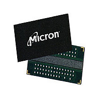
MT47H16M16BG-37E IT:B Micron Technology Inc, MT47H16M16BG-37E IT:B Datasheet - Page 11

MT47H16M16BG-37E IT:B
Manufacturer Part Number
MT47H16M16BG-37E IT:B
Description
Manufacturer
Micron Technology Inc
Type
DDR2 SDRAMr
Datasheet
1.MT47H16M16BG-37E_ITB.pdf
(128 pages)
Specifications of MT47H16M16BG-37E IT:B
Organization
16Mx16
Density
256Mb
Address Bus
15b
Access Time (max)
500ps
Maximum Clock Rate
533MHz
Operating Supply Voltage (typ)
1.8V
Package Type
FBGA
Operating Temp Range
-40C to 85C
Operating Supply Voltage (max)
1.9V
Operating Supply Voltage (min)
1.7V
Supply Current
180mA
Pin Count
84
Mounting
Surface Mount
Operating Temperature Classification
Industrial
Lead Free Status / Rohs Status
Compliant
- Current page: 11 of 128
- Download datasheet (10Mb)
Functional Block Diagrams
Figure 3: 64 Meg x 4 Functional Block Diagram
PDF: 09005aef8117c187
256MbDDR2.pdf - Rev. M 7/09 EN
BA0–BA1
A0–A12,
RAS#
CAS#
ODT
WE#
CKE
CK#
CS#
CK
15
Address
register
registers
Control
Mode
logic
15
Refresh
counter
13
11
2
The DDR2 SDRAM is a high-speed CMOS, dynamic random access memory. It is inter-
nally configured as a multibank DRAM.
13 Row-
address
MUX
2
Column-
counter/
control
address
Bank
logic
latch
13
latch and
decoder
address
Bank 0
row-
Bank 1
Bank 2
Bank 3
9
2
8,192
DM mask logic
(8,192 x 512 x 16)
Sense amplifiers
I/O gating
decoder
Column
8,192
memory
Bank 1
Bank 0
Bank 2
array
(x16)
Bank 3
512
Column 0, Column 1
16
Internal
CK, CK#
11
16
16
READ
latch
CK out
drivers
WRITE
FIFO
and
Column 0, Column 1
CK in
4
4
4
4
Micron Technology, Inc. reserves the right to change products or specifications without notice.
Mask
Data
MUX
16
4
generator
DQS
1
1
1
1
4
4
4
4
256Mb: x4, x8, x16 DDR2 SDRAM
registers
Input
Data
4
1
1
1
1
4
4
4
4
DQS, DQS#
2
1
4
CK, CK#
DRVRS
Functional Block Diagrams
2
DLL
RCVRS
sw1 sw2
sw1 sw2
sw1 sw2
sw1 sw2
R1
R1
R1
R1
R1
R1
©2003 Micron Technology, Inc. All rights reserved.
ODT control
R2
R2
R2
R2
R2
R2
VssQ
sw3
sw3
sw3
sw3
R3
R3
R3
R3
R3
R3
V
dd
Q
DQ0–DQ3
DQS, DQS#
DM
Related parts for MT47H16M16BG-37E IT:B
Image
Part Number
Description
Manufacturer
Datasheet
Request
R

Part Number:
Description:
IC DDR2 SDRAM 256MBIT 5NS 84FBGA
Manufacturer:
Micron Technology Inc
Datasheet:

Part Number:
Description:
IC DDR2 SDRAM 256MBIT 84FBGA
Manufacturer:
Micron Technology Inc
Datasheet:

Part Number:
Description:
IC DDR2 SDRAM 256MBIT 3NS 84FBGA
Manufacturer:
Micron Technology Inc
Datasheet:

Part Number:
Description:
IC DDR2 SDRAM 256MBIT 5NS 84FBGA
Manufacturer:
Micron Technology Inc
Datasheet:

Part Number:
Description:
IC DDR2 SDRAM 256MBIT 3NS 84FBGA
Manufacturer:
Micron Technology Inc
Datasheet:

Part Number:
Description:
IC DDR2 SDRAM 256MBIT 84FBGA
Manufacturer:
Micron Technology Inc

Part Number:
Description:
IC DDR2 SDRAM 256MBIT 3NS 84FBGA
Manufacturer:
Micron Technology Inc
Datasheet:

Part Number:
Description:
Manufacturer:
Micron Technology Inc
Datasheet:

Part Number:
Description:
Manufacturer:
Micron Technology Inc
Datasheet:

Part Number:
Description:
Manufacturer:
Micron Technology Inc
Datasheet:

Part Number:
Description:
Manufacturer:
Micron Technology Inc
Datasheet:

Part Number:
Description:
Manufacturer:
Micron Technology Inc
Datasheet:

Part Number:
Description:
IC SDRAM 64MBIT 133MHZ 54TSOP
Manufacturer:
Micron Technology Inc
Datasheet:

Part Number:
Description:
IC SDRAM 64MBIT 5.5NS 86TSOP
Manufacturer:
Micron Technology Inc
Datasheet:

Part Number:
Description:
IC SDRAM 64MBIT 200MHZ 86TSOP
Manufacturer:
Micron Technology Inc
Datasheet:


