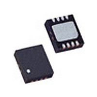
LTC2912IDDB-1#PBF Linear Technology, LTC2912IDDB-1#PBF Datasheet - Page 9

LTC2912IDDB-1#PBF
Manufacturer Part Number
LTC2912IDDB-1#PBF
Description
Manufacturer
Linear Technology
Datasheet
1.LTC2912IDDB-1PBF.pdf
(12 pages)
Specifications of LTC2912IDDB-1#PBF
Voltage Supervisor Type
Voltage Monitor
Number Of Voltage Supervisors
1
Monitored Supervisor Voltage
3.3
Reset Threshold Voltage (min)
AdjV
Reset Threshold Voltage (max)
AdjV
Operating Supply Voltage (min)
2.3V
Operating Supply Voltage (max)
6V
Operating Temperature Classification
Industrial
Operating Temp Range
-40C to 85C
Pin Count
8
Mounting
Surface Mount
Lead Free Status / Rohs Status
Compliant
Available stocks
Company
Part Number
Manufacturer
Quantity
Price
APPLICATIONS INFORMATION
When the VH input drops below its designed threshold,
the UV pin asserts low. When the input recovers above
its designed threshold, the UV output timer starts. If the
input remains above the designed threshold when the
timer fi nishes, the UV pin weakly pulls high. However, if
the input falls below its designed threshold during this
timeout period, the timer resets and restarts when the
input is above the designed threshold. The OV and OV
outputs behave as the UV output when LATCH is high
(LTC2912-1, LTC2912-3).
Selecting the UV/OV Timing Capacitor
The UV and OV timeout period (t
is adjustable to accommodate a variety of applications.
Connecting a capacitor, C
ground sets the timeout period. The value of capacitor
needed for a particular timeout period is:
The Reset Timeout Period vs Capacitance graph found in
the Typical Performance Characteristics shows the desired
delay time as a function of the value of the timer capacitor
that must be used. The TMR pin must have a minimum
10pF load or be tied to V
only limitation is the availability of a large value capaci-
tor with low leakage. Capacitor leakage current must not
exceed the minimum TMR charging current of 1.3μA.Tying
the TMR pin to V
Undervoltage Lockout
When V
undervoltage lockout (UVLO) condition. During UVLO, UV
is asserted and pulled low while OV and OV are cleared
and blocked from asserting. When V
follows the same timing procedure as an undervoltage
condition on the VH input.
Shunt Regulator
The LTC2912 has an internal shunt regulator. The V
operates as a direct supply input for voltages up to 6V. Under
this condition, the quiescent current of the device remains
below a maximum of 70μA. For V
6V, the device operates as a shunt regulator and should
C
TMR
= t
CC
UOTO
falls below 2V, the LTC2912 asserts an
• 115 • 10
CC
bypasses the timeout period.
CC
TMR
. For long timeout periods, the
–9
, between the TMR pin and
[F/s]
CC
UOTO
CC
voltages higher than
rises above 2V, UV
) for the LTC2912
CC
pin
have a resistance R
to limit the current to no greater than 10mA.
When choosing this resistance value, select an appropriate
location on the I-V curve shown in the Typical Performance
Characteristics to accommodate any variations in V
to changes in current through R
UV, OV and OV Output Characteristics
The DC characteristics of the UV, OV and 0V pull-up and
pull-down strength are shown in the Typical Performance
Characteristics. Each pin has a weak internal pull-up to
V
allows these pins to have open-drain behavior while pos-
sessing several other benefi cial characteristics. The weak
pull-up eliminates the need for an external pull-up resistor
when the rise time on the pin is not critical. On the other
hand, the open-drain confi guration allows for wired-OR
connections, and is useful when more than one signal
needs to pull down on the output. V
a maximum V
At V
on. Therefore, an external pull-up resistor of no more than
100k is recommended on the OV pin if the state and pull-up
strength of the OV pin is crucial at very low V
Note however, by adding an external pull-up resistor, the
pull-up strength on the OV pin is increased. Therefore, if
it is connected in a wired-OR connection, the pull-down
strength of any single device must accommodate this
additional pull-up strength.
Output Rise and Fall Time Estimation
The UV, OV and OV outputs have strong pull-down capa-
bility. The following formula estimates the output fall time
(90% to 10%) for a particular external load capacitance
(C
where R
transistor, typically 50Ω at V
perature (25°C). C
on the pin. Assuming a 150pF load capacitance, the fall
time is 16.5ns.
CC
LOAD
t
FALL
CC
and a strong pull-down to ground. This arrangement
= 1V, the weak pull-up current on OV is barely turned
):
≈ 2.2 • R
PD
is the on-resistance of the internal pull-down
OL
= 0.15V at UV.
PD
LOAD
Z
• C
between the supply and the V
LOAD
is the external load capacitance
CC
Z
> 1V and at room tem-
.
CC
LTC2912
of 1V guarantees
CC
.
CC
CC
9
due
2912fa
pin


