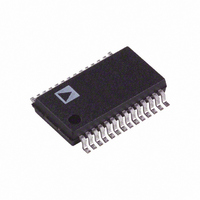
AD7564BRS Analog Devices Inc, AD7564BRS Datasheet - Page 3

AD7564BRS
Manufacturer Part Number
AD7564BRS
Description
IC DAC 12BIT LC2MOS QUAD 28-SSOP
Manufacturer
Analog Devices Inc
Datasheet
1.AD7564BRSZ.pdf
(16 pages)
Specifications of AD7564BRS
Mounting Type
Surface Mount
Rohs Status
RoHS non-compliant
Settling Time
500ns
Number Of Bits
12
Data Interface
Serial
Number Of Converters
4
Voltage Supply Source
Single Supply
Power Dissipation (max)
50µW
Operating Temperature
-40°C ~ 85°C
Package / Case
28-SSOP
Resolution (bits)
12bit
No. Of Pins
28
Peak Reflow Compatible (260 C)
No
Update Rate
1.8MSPS
No. Of Bits
12 Bit
Leaded Process Compatible
No
Interface Type
Serial
Lead Free Status / RoHS Status
Contains lead / RoHS non-compliant
Available stocks
Company
Part Number
Manufacturer
Quantity
Price
Part Number:
AD7564BRS
Manufacturer:
ADI/亚德诺
Quantity:
20 000
Part Number:
AD7564BRS-B
Manufacturer:
ADI/亚德诺
Quantity:
20 000
Company:
Part Number:
AD7564BRSZ
Manufacturer:
Maxim
Quantity:
456
Part Number:
AD7564BRSZ
Manufacturer:
ADI/亚德诺
Quantity:
20 000
Part Number:
AD7564BRSZ-REEL
Manufacturer:
ADI/亚德诺
Quantity:
20 000
Biased Mode
Parameter
ACCURACY
DIGITAL INPUTS
DIGITAL OUTPUT (SDOUT)
POWER REQUIREMENTS
NOTES
1
2
3
Specifications subject to change without notice.
(for example: AD7564AR-B). Figure 19 is an example of Biased Mode Operation.
These specifications apply with the devices biased up at 1.23 V for single supply applications. The model numbering reflects this by means of a "-B" suffix
Temperature ranges is as follows: A Version: –40 C to +85 C.
Not production tested. Guaranteed by characterization at initial product release.
Resolution
Relative Accuracy
Differential Nonlinearity
Gain Error
Gain Temperature Coefficient
Output Leakage Current
Input Resistance
V
V
V
V
I
C
Output Low Voltage (V
Output Low Voltage (V
Output High Voltage (V
Output High Voltage (V
V
Power Supply Sensitivity
I
INH
DD
INH
INH
INL
INL
DD
IN
REV. A
+25 C
T
I
@ +25 C
T
@ I
OUT1
, Input Capacitance
Gain/ V
MIN
MIN
, Input Current
, Input Low Voltage @ V
, Input Low Voltage @ V
, Input High Voltage @ V
, Input High Voltage @ V
Range
OUT2
to T
to T
Pins
DD
MAX
MAX
1
(V
T
MAX
DD
3
OL
OL
, unless otherwise noted)
OH
OH
= +3 V to +5.5 V; V
3
)
)
)
)
DD
DD
3
DD
DD
= +5 V
= +3.3 V
= +5 V
= +3.3 V
IOUT1
= V
A Grade
12
2
5
10
50
6
2.4
2.1
0.8
0.6
10
0.4
0.2
4.0
V
3/5.5
–75
10
IOUT2
1
0.9
4
5
1
DD
= 1.23 V; AGND = 0 V; V
– 0.2
2
Units
Bits
LSB max
LSB max
LSBs max
LSBs max
ppm FSR/ C typ
ppm FSR/ C max
nA max
nA max
k min
V min
V min
V max
V max
pF max
V max
V max
V min
V min
V min/V max
dB typ
A max
A max
–3–
REF
= 0 V to 2.45 V; T
Test Conditions/Comments
1 LSB = (V
V
All Grades Guaranteed Monotonic Over
Temperature
See Terminology Section
This Varies with DAC Input Code
Load Circuit as in Figure 2.
V
V
V
V
V
SDOUT Open Circuit
I
V
SDOUT Open Circuit
DD
IOUT2
DD
DD
DD
DD
INH
INH
is typically 2 mA with V
= +5 V
= +3.3 V
= +5 V
= +3.3 V
= V
= 2.4 V min, V
= 1.23 V and V
A
DD
= T
IOUT2
– 0.1 V min, V
MIN
to
– V
REF
INL
REF
)/2
= 0.8 V max;
12
= 0 V
INL
DD
= 300 V when
= 0.1 V max;
= +5 V,
AD7564


