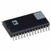
AD669AR Analog Devices Inc, AD669AR Datasheet - Page 3

AD669AR
Manufacturer Part Number
AD669AR
Description
IC DAC 16BIT MONO W/VREF 28-SOIC
Manufacturer
Analog Devices Inc
Series
DACPORT®r
Datasheet
1.AD669ANZ.pdf
(12 pages)
Specifications of AD669AR
Rohs Status
RoHS non-compliant
Settling Time
10µs
Number Of Bits
16
Data Interface
Parallel
Number Of Converters
1
Voltage Supply Source
Dual ±
Power Dissipation (max)
625mW
Operating Temperature
-40°C ~ 85°C
Mounting Type
Surface Mount
Package / Case
28-SOIC (7.5mm Width)
Number Of Channels
1
Resolution
16b
Conversion Rate
167KSPS
Interface Type
Parallel
Single Supply Voltage (typ)
Not RequiredV
Dual Supply Voltage (typ)
±15V
Power Supply Requirement
Dual
Output Type
Voltage
Single Supply Voltage (min)
Not RequiredV
Single Supply Voltage (max)
Not RequiredV
Dual Supply Voltage (min)
±13.5V
Dual Supply Voltage (max)
±16.5V
Operating Temp Range
-40C to 85C
Operating Temperature Classification
Industrial
Mounting
Surface Mount
Pin Count
28
Package Type
SOIC W
Lead Free Status / Rohs Status
Not Compliant
Available stocks
Company
Part Number
Manufacturer
Quantity
Price
Company:
Part Number:
AD669ARZ
Manufacturer:
MAXIM
Quantity:
12 040
Part Number:
AD669ARZ
Manufacturer:
ADI/亚德诺
Quantity:
20 000
REV. A
AC PERFORMANCE CHARACTERISTICS
Ratio, these characteristics are included for design guidance only and are not subject to test. THD+N and SNR are 100% tested.
T
Parameter
Output Settling Time
Total Harmonic Distortion + Noise
Signal-to-Noise Ratio
Digital-to-Analog Glitch Impulse
Digital Feedthrough
Output Noise Voltage
Reference Noise
Specifications subject to change without notice.
Specifications in boldface are tested on all production units at final electrical test. Results from those tests are used to calculate outgoing quality levels. All min and
max specifications are guaranteed. Those shown in boldface are tested on all production units.
TIMING CHARACTERISTICS
V
Parameter
(Figure la)
t
t
t
t
t
t
(Figure lb)
t
t
t
t
Specifications subject to change without notice.
Specifications in boldface are tested on all production units at final electrical
test. Results from those tests are used to calculate outgoing quality levels. All
min and max specifications are guaranteed. Those shown in boldface are tested
on all production units.
CS
LI
DS
DH
LH
LW
LOW
HIGH
DS
DH
MIN
CC
(Time to 0.0008% FS
with 2 k , 1000 pF Load)
A, B, S Grade
A, B, S Grade
A, B, S Grade
Density (1 kHz – 1 MHz)
= +15 V, V
T
A
T
MAX
EE
, V
= –15 V, V
Limit
+25 C
40
40
30
10
90
40
130
40
120
10
CC
= +15 V, V
LL
= +5 V, V
EE
Limit
–40 C to
+85 C
50
50
35
10
110
45
150
45
140
10
= –15 V, V
HI
= 2.4 V, V
LL
Limit
13
8
10
6
8
2.5
0.009
0.07
7.0
83
15
2
120
125
= +5 V except where noted.)
Limit
–55 C to
+125 C
55
55
40
15
120
45
165
45
150
15
LO
= 0.4 V
Units
% max
% max
% max
dB min
nV-s typ
nV-s typ
nV/ Hz typ
nV/ Hz typ
s max
s typ
s typ
s typ
s typ
s typ
Units
ns min
ns min
ns min
ns min
ns min
ns min
ns min
ns min
ns min
ns min
(With the exception of Total Harmonic Distortion + Noise and Signal-to-Noise
–3–
Test Conditions/Comments
20 V Step, T
20 V Step, T
20 V Step, T
10 V Step, T
10 V Step, T
1 LSB Step, T
0 dB, 1001 Hz; Sample Rate = 100 kHz; T
–20 dB, 1001 Hz; Sample Rate = 100 kHz; T
–60 dB, 1001 Hz; Sample Rate = 100 kHz; T
T
DAC Alternately Loaded with 8000H and 7FFFH
DAC Alternately Loaded with 0000H and FFFFH; CS High
Measured at V
Measured at REF OUT
A
DATA
LDAC
= +25 C
Figure 1a. AD669 Level Triggered Timing Diagram
Figure 1b. AD669 Edge Triggered Timing Diagram
CS
L1
CS AND/OR
TIE CS AND/OR L1 TO GROUND OR TOGETHER WITH LDAC
L1, LDAC
DATA
A
A
MIN
A
MIN
MIN
= +25 C
= +25 C
= +25 C
OUT
, 20 V Span; Excludes Reference
T
T
t
T
t
A
A
CS
L1
t
A
DS
T
T
T
MAX
MAX
MAX
t
DH
t
LOW
t
DS
t
t
LH
DH
t
HIGH
A
= +25 C
A
A
= +25 C
= +25 C
AD669
t
LW


