LM4960SQ National Semiconductor, LM4960SQ Datasheet - Page 8
LM4960SQ
Manufacturer Part Number
LM4960SQ
Description
AMP, FOR CERAMSPEAKER, MINI SOIC8
Manufacturer
National Semiconductor
Datasheet
1.LM4960SQ.pdf
(12 pages)
Specifications of LM4960SQ
Operational Class
Class-AB
Audio Amplifier Output Configuration
1-Channel Mono
Audio Amplifier Function
Speaker
Total Harmonic Distortion
0.04@20Ohm%
Single Supply Voltage (typ)
3/5V
Dual Supply Voltage (typ)
Not RequiredV
Power Supply Requirement
Single
Rail/rail I/o Type
No
Power Supply Rejection Ratio
60dB
Single Supply Voltage (min)
3V
Single Supply Voltage (max)
7V
Dual Supply Voltage (min)
Not RequiredV
Dual Supply Voltage (max)
Not RequiredV
Operating Temp Range
-40C to 85C
Operating Temperature Classification
Industrial
Mounting
Surface Mount
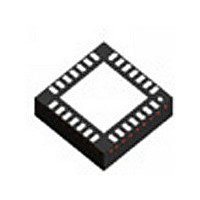
Pin Count
28
No. Of Channels
1
Supply Voltage Range
3V To 7V
Thd + N
0.04% @ 3W, VDD=5V
Load Impedance
20ohm
Operating Temperature Range
-40°C To +85°C
Amplifier Case Style
LLP
No. Of Pins
28
Svhc
No SVHC
Rohs Compliant
Yes
Lead Free Status / Rohs Status
Not Compliant
Available stocks
Company
Part Number
Manufacturer
Quantity
Price
Company:

Part Number:
LM4960SQ
Manufacturer:
PH
Quantity:
4 416
Company:
Part Number:
LM4960SQ/NOPB
Manufacturer:
NS
Quantity:
339


www.national.com
Application Information
BRIDGE CONFIGURATION EXPLANATION
The Audio Amplifier portion of the LM4960 has two internal
amplifiers allowing different amplifier configurations. The first
amplifier’s gain is externally configurable, whereas the sec-
ond amplifier is internally fixed in a unity-gain, inverting
configuration. The closed-loop gain of the first amplifier is set
by selecting the ratio of Rf to Ri while the second amplifier’s
gain is fixed by the two internal 20kΩ resistors. Figure 1
shows that the output of amplifier one serves as the input to
amplifier two. This results in both amplifiers producing sig-
nals identical in magnitude, but out of phase by 180˚. Con-
sequently, the differential gain for the Audio Amplifier is
By driving the load differentially through outputs Vo1 and
Vo2, an amplifier configuration commonly referred to as
“bridged mode” is established. Bridged mode operation is
different from the classic single-ended amplifier configura-
tion where one side of the load is connected to ground.
A bridge amplifier design has a few distinct advantages over
the single-ended configuration. It provides differential drive
to the load, thus doubling the output swing for a specified
supply voltage. Four times the output power is possible as
compared to a single-ended amplifier under the same con-
ditions. This increase in attainable output power assumes
that the amplifier is not current limited or clipped. In order to
choose an amplifier’s closed-loop gain without causing ex-
cessive clipping, please refer to the Audio Power Amplifier
Design section.
The bridge configuration also creates a second advantage
over single-ended amplifiers. Since the differential outputs,
Vo1 and Vo2, are biased at half-supply, no net DC voltage
exists across the load. This eliminates the need for an output
coupling capacitor which is required in a single supply,
single-ended amplifier configuration. Without an output cou-
pling capacitor, the half-supply bias across the load would
result in both increased internal IC power dissipation and
also possible loudspeaker damage.
AMPLIFIER POWER DISSIPATION
Power dissipation is a major concern when designing a
successful amplifier, whether the amplifier is bridged or
single-ended. A direct consequence of the increased power
delivered to the load by a bridge amplifier is an increase in
internal power dissipation. Since the amplifier portion of the
LM4960 has two operational amplifiers, the maximum inter-
nal power dissipation is 4 times that of a single-ended am-
plifier. The maximum power dissipation for a given BTL
application can be derived from Equation 1.
where
P
DMAX(AMP)
Z
L
= R
A
VD
o
1 + R
= 4(V
= 2 *(Rf/Ri)
o
DD
2 +1/2πfc
)
2
/ (2π
2
Z
L
)
(1)
8
BOOST CONVERTER POWER DISSIPATION
At higher duty cycles, the increased ON-time of the switch
FET means the maximum output current will be determined
by power dissipation within the LM2731 FET switch. The
switch power dissipation from ON-time conduction is calcu-
lated by Equation 2.
where DC is the duty cycle.
There will be some switching losses as well, so some derat-
ing needs to be applied when calculating IC power dissipa-
tion.
TOTAL POWER DISSIPATION
The total power dissipation for the LM4960 can be calculated
by adding Equation 1 and Equation 2 together to establish
Equation 3:
The result from Equation 3 must not be greater than the
power dissipation that results from Equation 4:
For the LQA28A, θ
LM4960. Depending on the ambient temperature, T
system surroundings, Equation 4 can be used to find the
maximum internal power dissipation supported by the IC
packaging. If the result of Equation 3 is greater than that of
Equation 4, then either the supply voltage must be in-
creased, the load impedance increased or T
the typical application of a 3V power supply, with V1 set to
12V and a 800nF + 20Ω load, the maximum ambient tem-
perature possible without violating the maximum junction
temperature is approximately 118˚C provided that device
operation is around the maximum power dissipation point.
Thus, for typical applications, power dissipation is not an
issue. Power dissipation is a function of output power and
thus, if typical operation is not around the maximum power
dissipation point, the ambient temperature may be increased
accordingly. Refer to the Typical Performance Characteris-
tics curves for power dissipation information for lower output
levels.
EXPOSED-DAP PACKAGE PCB MOUNTING
CONSIDERATIONS
The LM4960’s exposed-DAP (die attach paddle) package
(LD) provides a low thermal resistance between the die and
the PCB to which the part is mounted and soldered. The low
thermal resistance allows rapid heat transfer from the die to
the surrounding PCB copper traces, ground plane, and sur-
rounding air. The LD package should have its DAP soldered
to a copper pad on the PCB. The DAP’s PCB copper pad
may be connected to a large plane of continuous unbroken
copper. This plane forms a thermal mass, heat sink, and
radiation area. Further detailed and specific information con-
cerning PCB layout, fabrication, and mounting an LD (LLP)
package is found in National Semiconductor’s Package En-
gineering Group under application note AN1187.
P
DMAX(TOTAL)
P
DMAX(SWITCH)
= [4*(V
P
DMAX
JA
DD
= DC x I
= (T
= 59˚C/W. T
)
2
/2π
S
JMAX
(ON)]
2
Z
IND
L
] + [DC x I
- T
(AVE)
A
JMAX
) / θJA
2
x R
= 125˚C for the
IND
A
DS
(AVE)
reduced. For
(ON)
A
2
, of the
xR
D -
(2)
(3)
(4)
Related parts for LM4960SQ
Image
Part Number
Description
Manufacturer
Datasheet
Request
R

Part Number:
Description:
National Semiconductor [8-Bit D/A Converter]
Manufacturer:
National Semiconductor
Datasheet:
Part Number:
Description:
National Semiconductor [Media Coprocessor]
Manufacturer:
National Semiconductor
Datasheet:
Part Number:
Description:
Digitally Controlled Tone and Volume Circuit with Stereo Audio Power Amplifier, Microphone Preamp Stage and National 3D Sound
Manufacturer:
National Semiconductor
Datasheet:
Part Number:
Description:
Digitally Controlled Tone and Volume Circuit with Stereo Audio Power Amplifier, Microphone Preamp Stage and National 3D Sound
Manufacturer:
National Semiconductor
Datasheet:
Part Number:
Description:
AC97 Rev 2 Codec with Sample Rate Conversion and National 3D Sound
Manufacturer:
National Semiconductor
Part Number:
Description:
Manufacturer:
National Semiconductor
Datasheet:
Part Number:
Description:
Manufacturer:
National Semiconductor
Datasheet:
Part Number:
Description:
General Purpose, Low Voltage, Low Power, Rail-to-Rail Output Operational Amplifiers
Manufacturer:
National Semiconductor
Datasheet:
Part Number:
Description:
8-bit 20 MSPS flash A/D converter.
Manufacturer:
National Semiconductor
Datasheet:
Part Number:
Description:
Low Noise Quad Operational Amplifier
Manufacturer:
National Semiconductor
Datasheet:
Part Number:
Description:
Quad Differential Line Receivers
Manufacturer:
National Semiconductor
Datasheet:
Part Number:
Description:
Quad High Speed Trapezoidal? Bus Transceiver
Manufacturer:
National Semiconductor
Datasheet:
Part Number:
Description:
Dual Line Receiver
Manufacturer:
National Semiconductor
Datasheet:
Part Number:
Description:
TTL to 10k ECL Level Translator with Latch
Manufacturer:
National Semiconductor
Datasheet: