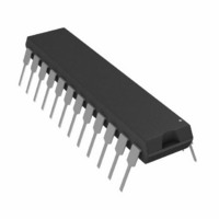
AD7237KN Analog Devices Inc, AD7237KN Datasheet - Page 10

AD7237KN
Manufacturer Part Number
AD7237KN
Description
IC DAC 12BIT LC2MOS DUAL 24-DIP
Manufacturer
Analog Devices Inc
Series
DACPORT®r
Specifications of AD7237KN
Data Interface
Parallel
Rohs Status
RoHS non-compliant
Settling Time
8µs
Number Of Bits
12
Number Of Converters
2
Voltage Supply Source
Dual ±
Operating Temperature
-40°C ~ 85°C
Mounting Type
Through Hole
Package / Case
24-DIP (0.300", 7.62mm)
Resolution (bits)
12bit
Sampling Rate
125kSPS
Input Channel Type
Parallel
Supply Current
11mA
Digital Ic Case Style
DIP
No. Of Pins
24
Current, Supply
± 10 μA (Max.)
Differential Nonlinearity
± 0.9 LSB (Min.)
Offset Error
± 3 LBS (Max.)
Package Type
PDIP
Power Dissipation
1000 mW
Resolution
12 Bits
Temperature, Operating, Maximum
85 °C
Temperature, Operating, Minimum
-40 °C
Voltage, Input Range
5.25 V (Max.) (Ref.)
Voltage, Supply
2.4 V (Min.)
Power Dissipation (max)
-
Lead Free Status / RoHS Status
Contains lead / RoHS non-compliant
AD7237A/AD7247A
APPLYING THE AD7237A/AD7247A
The internal scaling resistors provided on the AD7237A/
AD7247A allow several output voltage ranges. The part can
produce unipolar output ranges of 0 V to +5 V or 0 V to +10 V
and a bipolar output range of 5 V. Connections for the various
ranges are outlined below. Since each DAC has its own R
input the two DACs on each part can be set up for different
output ranges.
Unipolar (0 V to +10 V) Configuration
The first of the configurations provides an output voltage range
of 0 V to +10 V. This is achieved by connecting the output off-
set resistor, R
In this configuration, the AD7237A/AD7247A can be operated
from single or dual supplies. Figure 8 shows the connection dia-
gram for unipolar operation for DAC A of the AD7237A, while
the table for output voltage versus digital code in the DAC latch
is shown in Table III. Similar connections apply to the AD7247A.
DAC Latch Contents
MSB
1111 1111 1111
1000 0000 0001
1000 0000 0000
0111 1111 1111
0000 0000 0001
0000 0000 0000
Note: 1 LSB = REF IN/2048.
Table III. Unipolar Code Table (0 to +10 V Range)
Figure 8. Unipolar (0 to +10 V) Configuration
LSB
OFSA
, or R
OFSB
Analog Output, V
+2 • REF IN (4095/4096)
+2 • REF IN (2049/4096)
+2 • REF IN (2048/4096) = +REF IN
+2 • REF IN (2047/4096)
+2 • REF IN (1/4096)
0 V
, to AGND (GND for AD7247A).
OUT
OFS
–10–
Unipolar (0 V to +5 V) Configuration
The 0 V to +5 V output voltage range is achieved by tying R
or R
AD7247A can be operated single supply or from dual supplies.
The table for output voltage versus digital code is as in Table
III, with 2 • REF IN replaced by REF IN. Note, for this range,
1 LSB = REF IN • (2
Bipolar Configuration
The bipolar configuration for the AD7237A/AD7247A, which
gives an output range of –5 V to +5 V, is achieved by connect-
ing R
be operated from dual supplies to achieve this output voltage
range. Figure 9 shows the connection diagram for bipolar opera-
tion for DAC A of the AD7247A. An AD586 provides the refer-
ence voltage for the DAC but this could be provided by the
on-chip reference by connecting REF OUT to REF IN. The
code table for bipolar operation is shown in Table IV. Similar
connections apply for the AD7237A.
DAC Latch Contents
MSB
1111 1111 1111
1000 0000 0001
1000 0000 0000
0111 1111 1111
0000 0000 0001
0000 0000 0000
Note: 1 LSB = REF IN/2048.
OFSB
OFSA
to V
, or R
LSB
OUTA
Figure 9. Bipolar Configuration
OFSB
Table IV. Bipolar Code Table
or V
, to REF IN. The AD7237A/AD7247A must
–12
OUTB
) = (REF IN/4096).
. Once again, the AD7237A/
Analog Output, V
+REF IN • (2047/2048)
+REF IN • (1/2048)
0 V
–REF IN • (1/2048)
–REF IN • (2047/2048)
–REF IN • (2048/2048) = –REF IN
OUT
REV. 0
OFSA


