Î Î Î Î Î Î Î Î Î Î Î Î Î Î Î Î Î Î Î Î Î Î Î
Î Î Î Î Î Î Î Î Î Î Î Î Î Î Î Î Î Î Î Î Î Î Î
Î Î Î Î Î Î Î Î Î Î Î
Î Î Î Î Î Î Î Î Î Î Î Î Î Î Î Î Î Î Î Î Î Î Î
Î Î Î Î Î Î Î Î Î Î Î
Î Î Î Î Î Î Î Î Î Î Î Î Î Î Î Î Î Î Î Î Î Î Î
Î Î Î Î Î Î Î Î Î Î Î
Î Î Î Î Î Î Î Î Î Î Î
Î Î Î Î Î Î Î Î Î Î Î
Î Î Î Î Î Î Î Î Î Î Î
Î Î Î Î Î Î Î Î Î Î Î
Î Î Î Î Î Î Î Î Î Î Î
Î Î Î Î Î Î Î Î Î Î Î
Î Î Î Î Î Î Î Î Î Î Î
Î Î Î Î Î Î Î Î Î Î Î
Î Î Î Î Î Î Î Î Î Î Î
Î Î Î Î Î Î Î Î Î Î Î
Î Î Î Î Î Î Î Î Î Î Î
Î Î Î Î Î Î Î Î Î Î Î
Î Î Î Î Î Î Î Î Î Î Î
Î Î Î Î Î Î Î Î Î Î Î
Î Î Î Î Î Î Î Î Î Î Î
Î Î Î Î Î Î Î Î Î Î Î
Î Î Î Î Î Î Î Î Î Î Î
Î Î Î Î Î Î Î Î Î Î Î
Î Î Î Î Î Î Î Î Î Î Î
Î Î Î Î Î Î Î Î Î Î Î
Î Î Î Î Î Î Î Î Î Î Î
Î Î Î Î Î Î Î Î Î Î Î
Î Î Î Î Î Î Î Î Î Î Î
Î Î Î Î Î Î Î Î Î Î Î
Î Î Î Î Î Î Î Î Î Î Î
Î Î Î Î Î Î Î Î Î Î Î
Î Î Î Î Î Î Î Î Î Î Î
Î Î Î Î Î Î Î Î Î Î Î
Î Î Î Î Î Î Î Î Î Î Î
Î Î Î Î Î Î Î Î Î Î Î
Î Î Î Î Î Î Î Î Î Î Î Î Î Î Î Î Î Î Î Î Î Î Î
Î Î Î Î Î Î Î Î Î Î Î
Î Î Î Î Î Î Î Î Î Î Î Î Î Î Î Î Î Î Î Î Î Î Î
Î Î Î Î Î Î Î Î Î Î Î Î
Î Î Î Î Î Î Î Î Î Î Î
Î Î Î Î Î Î Î Î Î Î Î Î Î Î Î Î Î Î Î Î Î Î Î
Î Î Î Î Î Î Î Î Î Î Î Î
Î Î Î Î Î Î Î Î Î Î Î Î
Î Î Î Î Î Î Î Î Î Î Î Î Î Î Î Î Î Î Î Î Î Î Î
Î Î Î Î Î Î Î Î Î Î Î Î
Î Î Î Î Î Î Î Î Î Î Î Î
Î Î Î Î Î Î Î Î Î Î Î Î
Î Î Î Î Î Î Î Î Î Î Î Î
Î Î Î Î Î Î Î Î Î Î Î Î
MOTOROLA
SEMICONDUCTOR TECHNICAL DATA
Darlington Complementary
Silicon Power Transistors
. . . designed for general–purpose amplifier and low–frequency switching applica-
tions.
* Indicates JEDEC Registered Data.
Preferred devices are Motorola recommended choices for future use and best overall value.
*MAXIMUM RATINGS
*THERMAL CHARACTERISTICS
Motorola Bipolar Power Transistor Device Data
Collector–Emitter Voltage
Collector–Base Voltage
Emitter–Base Voltage
Collector Current — Continuous
Base Current
Total Device Dissipation @ T C = 25 _ C
Operating and Storage Junction
Thermal Resistance, Junction to Case
Motorola, Inc. 1995
High DC Current Gain @ I C = 10 Adc —
Collector–Emitter Sustaining Voltage —
Monolithic Construction with Built–In Base–Emitter Shunt Resistors
Derate above 25 _ C
Temperature Range
h FE = 2400 (Typ) — 2N6282, 2N6283, 2N6284
h FE
V CEO(sus) = 60 Vdc (Min) — 2N6282, 2N6285
V CEO(sus)
V CEO(sus)
= 4000 (Typ) — 2N6285, 2N6286, 2N6287
Characteristic
Rating
= 80 Vdc (Min) — 2N6283, 2N6286
= 100 Vdc (Min) — 2N6284, 2N6287
Peak
140
120
100
160
80
60
40
20
0
0
Î Î Î Î
Î Î Î Î
Î Î Î Î
Î Î Î Î
Î Î Î Î
Î Î Î Î
Î Î Î Î
Î Î Î Î
Î Î Î Î
Î Î Î Î
Î Î Î Î
Î Î Î Î
Î Î Î Î
Î Î Î Î
Î Î Î Î
Î Î Î Î
Î Î Î Î
Î Î Î Î
Î Î Î Î
Î Î Î Î
Î Î Î Î
Î Î Î Î
Î Î Î Î
Î Î Î Î
Î Î Î Î
Î Î Î Î
Î Î Î Î
Î Î Î Î
Î Î Î Î
Î Î Î Î
Î Î Î Î
Î Î Î Î
Î Î Î Î
Î Î Î Î
Î Î Î Î
Symbol
Î Î Î Î Î
Î Î Î Î Î
Î Î Î Î Î
Î Î Î Î Î
Î Î Î Î Î
Î Î Î Î Î
Î Î Î Î Î
Î Î Î Î Î
T J ,T stg
25
V CEO
V CB
V EB
P D
I C
I B
Symbol
50
Figure 1. Power Derating
Î Î Î
Î Î Î
Î Î Î
Î Î Î
Î Î Î
Î Î Î
Î Î Î
Î Î Î
Î Î Î
Î Î Î
Î Î Î Î Î Î Î Î
Î Î Î
Î Î Î
Î Î Î Î Î Î Î Î
Î Î Î Î Î Î Î Î
Î Î Î
Î Î Î Î Î Î Î Î
Î Î Î Î Î Î Î Î
Î Î Î Î Î Î Î Î
Î Î Î Î Î Î Î Î
Î Î Î Î Î Î Î Î
Î Î Î Î Î Î Î Î
Î Î Î Î Î Î Î Î
Î Î Î Î Î Î Î Î
Î Î Î Î Î Î Î Î
Î Î Î Î Î Î Î Î
Î Î Î Î Î Î Î Î
Î Î Î Î Î Î Î Î
Î Î Î Î Î Î Î Î
Î Î Î Î Î Î Î Î
Î Î Î Î Î Î Î Î
Î Î Î Î Î Î Î Î
Î Î Î Î Î Î Î Î
Î Î Î Î Î Î Î Î
Î Î Î Î Î Î Î Î
R JC
T C , CASE TEMPERATURE ( C)
2N6282
2N6285
60
60
75
Î Î Î Î
Î Î Î Î
Î Î Î Î
Î Î Î Î
Î Î Î Î
Î Î Î Î
Î Î Î Î
Î Î Î Î
Î Î Î Î
Î Î Î Î
Î Î Î Î
Î Î Î Î
Î Î Î Î
Î Î Î Î Î Î
Î Î Î Î Î Î
Î Î Î Î Î Î
Î Î Î Î Î Î
Î Î Î Î Î Î
Î Î Î Î Î Î
Î Î Î Î Î Î
Î Î Î Î Î Î
– 65 to + 200
2N6283
2N6286
100
0.915
160
5.0
0.5
80
80
20
40
Max
1.09
125
Î Î Î
Î Î Î
Î Î Î
Î Î Î
Î Î Î
Î Î Î
Î Î Î
Î Î Î
Î Î Î
Î Î Î
Î Î Î
Î Î Î
Î Î Î
2N6284
2N6287
100
100
150
Î Î Î
Î Î Î
Î Î Î
Î Î Î
Î Î Î
Î Î Î
Î Î Î
Î Î Î
Î Î Î
Î Î Î
Î Î Î
Î Î Î
Î Î Î
Î Î Î
Î Î Î
Î Î Î
Î Î Î
Î Î Î
Î Î Î
Î Î Î
Î Î Î
Î Î Î
Î Î Î
Î Î Î
Î Î Î
Î Î Î
Î Î Î
Î Î Î
Î Î Î
Î Î Î
Î Î Î
Î Î Î
Î Î Î
Î Î Î
Î Î Î
Î Î Î
Î Î Î
Î Î Î
Î Î Î
Î Î Î
Î Î Î
Î Î Î
Î Î Î
_ C/W
Watts
W/ _ C
Unit
175
Unit
Vdc
Vdc
Vdc
Adc
Adc
_ C
200
POWER TRANSISTORS
COMPLEMENTARY
*Motorola Preferred Device
60, 80, 100 VOLTS
2N6282
2N6284
2N6285
2N6287
DARLINGTON
20 AMPERE
160 WATTS
Order this document
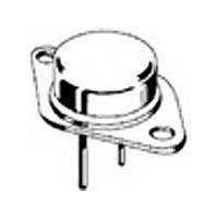
CASE 1–07
thru
thru
TO–204AA
SILICON
NPN
PNP
(TO–3)
by 2N6282/D
*
*
1