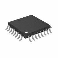
AD5764ASUZ Analog Devices Inc, AD5764ASUZ Datasheet - Page 24

AD5764ASUZ
Manufacturer Part Number
AD5764ASUZ
Description
IC DAC 16BIT QUAD VOUT 32-TQFP
Manufacturer
Analog Devices Inc
Datasheet
1.AD5764BSUZ.pdf
(28 pages)
Specifications of AD5764ASUZ
Data Interface
Serial
Design Resources
High Accuracy, Bipolar Voltage Output Digital-to-Analog Conversion Using AD5764 (CN0006)
Settling Time
8µs
Number Of Bits
16
Number Of Converters
4
Voltage Supply Source
Dual ±
Power Dissipation (max)
275mW
Operating Temperature
-40°C ~ 85°C
Mounting Type
Surface Mount
Package / Case
32-TQFP, 32-VQFP
Resolution (bits)
16bit
Sampling Rate
1.26MSPS
Input Channel Type
Serial
Supply Voltage Range - Digital
2.7V To 5.25V
Supply Current
3.5mA
Digital Ic Case Style
QFP
Lead Free Status / RoHS Status
Lead free / RoHS Compliant
For Use With
EVAL-AD5764EBZ - BOARD EVAL FOR AD5764
Lead Free Status / RoHS Status
Lead free / RoHS Compliant, Lead free / RoHS Compliant
Available stocks
Company
Part Number
Manufacturer
Quantity
Price
Company:
Part Number:
AD5764ASUZ
Manufacturer:
ADI
Quantity:
210
Company:
Part Number:
AD5764ASUZ
Manufacturer:
Analog Devices Inc
Quantity:
10 000
Company:
Part Number:
AD5764ASUZ-REEL7
Manufacturer:
Analog Devices Inc
Quantity:
10 000
AD5764
DESIGN FEATURES
ANALOG OUTPUT CONTROL
In many industrial process control applications, it is vital that
the output voltage be controlled during power-up and during
brownout conditions. When the supply voltages are changing,
the VOUTx pins are clamped to 0 V via a low impedance path.
To prevent the output amp being shorted to 0 V during this time,
Transmission Gate G1 is also opened (see Figure 35). These condi-
tions are maintained until the power supplies stabilize and a
valid word is written to the data register. At this time, G2 opens and
G1 closes. Both transmission gates are also externally controllable
via the reset logic ( RSTIN ) control input. For instance, if RSTIN
is driven from a battery supervisor chip, the RSTIN input is
driven low to open G1 and close G2 upon power-down or during
a brownout. Conversely, the on-chip voltage detector output
( RSTOUT ) is also available to the user to control other parts of
the system. The basic transmission gate functionality is shown
in
DIGITAL OFFSET AND GAIN CONTROL
The AD5764 incorporates a digital offset adjust function with a
±16 LSB adjust range and 0.125 LSB resolution. The coarse gain
register allows the user to adjust the AD5764 full-scale output
range. The full-scale output can be programmed to achieve full-
scale ranges of ±10 V, ±10.2564 V, and ±10.5263 V. A fine gain
trim is also provided.
Figure 35
CONTROL
VOLTAGE
MONITOR
.
AND
Figure 35. Analog Output Control Circuitry
RSTOUT
G1
G2
RSTIN
AGNDA
VOUTA
Rev. D | Page 24 of 28
PROGRAMMABLE SHORT-CIRCUIT PROTECTION
The short-circuit current of the output amplifiers can be pro-
grammed by inserting an external resistor between the ISCC
pin and PGND. The programmable range for the current is 500 μA
to 10 mA, corresponding to a resistor range of 120 kΩ to 6 kΩ.
The resistor value is calculated as follows:
If the ISCC pin is left unconnected, the short-circuit current
limit defaults to 5 mA. Note that limiting the short-circuit
current to a small value can affect the slew rate of the output
when driving into a capacitive load; therefore, the value of the
programmed short circuit should take into account the size of
the capacitive load being driven.
DIGITAL I/O PORT
The AD5764 contains a 2-bit digital I/O port (D1 and D0).
These bits can be configured as inputs or outputs independently,
and can be driven or have their values read back via the serial
interface. The I/O port signals are referenced to DV
When configured as outputs, they can be used as control signals
to multiplexers or can be used to control calibration circuitry
elsewhere in the system. When configured as inputs, the logic
signals from limit switches can, for example, be applied to D0
and D1 and can be read back via the digital interface.
LOCAL GROUND OFFSET ADJUST
The AD5764 incorporates a local ground offset adjust feature
that, when enabled in the function register, adjusts the DAC
outputs for voltage differences between the individual DAC ground
pins, AGNDx, and the REFGND pin, ensuring that the DAC
output voltages are always with respect to the local DAC ground
pin. For instance, if Pin AGNDA is at +5 mV with respect to the
REFGND pin and VOUTA is measured with respect to AGNDA,
a −5 mV error results, enabling the local ground offset adjust
feature to adjust VOUTA by +5 mV, eliminating the error.
R
=
I
60
S
C
CC
and DGND.


