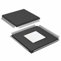
AD9779ABSVZ Analog Devices Inc, AD9779ABSVZ Datasheet - Page 41

AD9779ABSVZ
Manufacturer Part Number
AD9779ABSVZ
Description
IC DAC 16BIT 1.0GSPS 100TQFP
Manufacturer
Analog Devices Inc
Specifications of AD9779ABSVZ
Data Interface
Serial
Design Resources
Interfacing ADL5370 to AD9779A Dual-Channel, 1 GSPS High Speed DAC (CN0016) Interfacing ADL5371 to AD9779A Dual-Channel, 1 GSPS High Speed DAC (CN0017) Interfacing ADL5372 to AD9779A Dual-Channel, 1 GSPS High Speed DAC (CN0018) Interfacing ADL5373 to AD9779A Dual-Channel, 1 GSPS High Speed DAC (CN0019) Interfacing ADL5374 to AD9779A Dual-Channel, 1 GSPS High Speed DAC (CN0020) Interfacing ADL5375 to AD9779A Dual-Channel, 1 GSPS High Speed DAC (CN0021)
Number Of Bits
16
Number Of Converters
2
Voltage Supply Source
Analog and Digital
Power Dissipation (max)
300mW
Operating Temperature
-40°C ~ 85°C
Mounting Type
Surface Mount
Package / Case
100-TQFP Exposed Pad, 100-eTQFP, 100-HTQFP, 100-VQFP
Resolution (bits)
16bit
Sampling Rate
1GSPS
Input Channel Type
Parallel
Digital Ic Case Style
QFP
No. Of Pins
100
Operating Temperature Range
-40°C To +85°C
Number Of Channels
2
Resolution
16b
Interface Type
Parallel
Single Supply Voltage (typ)
3.3V
Dual Supply Voltage (typ)
Not RequiredV
Architecture
Interpolation Filter
Power Supply Requirement
Analog and Digital
Output Type
Current
Single Supply Voltage (min)
3.13V
Single Supply Voltage (max)
3.47V
Dual Supply Voltage (min)
Not RequiredV
Dual Supply Voltage (max)
Not RequiredV
Operating Temp Range
-40C to 85C
Operating Temperature Classification
Industrial
Mounting
Surface Mount
Pin Count
100
Package Type
TQFP EP
Lead Free Status / RoHS Status
Lead free / RoHS Compliant
For Use With
AD9779A-EBZ - BOARD EVALUATION FOR AD9779A
Settling Time
-
Lead Free Status / Rohs Status
Compliant
Available stocks
Company
Part Number
Manufacturer
Quantity
Price
Company:
Part Number:
AD9779ABSVZ
Manufacturer:
ADI
Quantity:
1
Company:
Part Number:
AD9779ABSVZ
Manufacturer:
ADI
Quantity:
184
Company:
Part Number:
AD9779ABSVZ
Manufacturer:
Analog Devices Inc
Quantity:
10 000
Part Number:
AD9779ABSVZ
Manufacturer:
ADI/亚德诺
Quantity:
20 000
Company:
Part Number:
AD9779ABSVZRL
Manufacturer:
Analog Devices Inc
Quantity:
10 000
LO FEEDTHROUGH COMPENSATION
The LO feedthrough compensation is the most complex of all
three operations. This is due to the structure of the offset aux-
iliary DACs, as shown in Figure 77. To achieve LO feedthrough
compensation in a circuit, each of four outputs of these AUX
DACs must be connected through a 50 Ω resistor to ground
and through a 250 Ω resistor to one of the four quadrature
modulator signal inputs. The purpose of these connections is
to drive a very small amount of current into the nodes at the
quadrature modulator inputs, therefore adding a slight dc bias
to one or the other of the quadrature modulator signal inputs.
This can be seen in the schematics for the AD9776A/AD9778A/
AD9779A evaluation board (see Figure 106).
To achieve LO feedthrough compensation, the user should start
with the default conditions of the AUX DAC sign registers, and
then increment the magnitude of one or the other AUX DAC
output currents. While this is being done, the amplitude of the
LO feedthrough at the quadrature modulator output should be
sensed. If the LO feedthrough amplitude increases, try either
changing the sign of the AUX DAC being adjusted, or adjusting
the output current of the other AUX DAC. It may take practice
before an effective algorithm is achieved.
AD9779A
25Ω TO 50Ω
I DAC
Figure 79. Typical Use of Auxiliary DACs DC Coupling to Quadrature
I OR Q DAC
AD9779A
Figure 78. Typical Use of Auxiliary DACs AC Coupling to
25Ω TO 50Ω
0.1µF
0.1µF
AD9779A
25Ω TO 50Ω
Q DAC
Modulator with DC Shift
FILTERING
OPTIONAL
Quadrature Modulator
PASSIVE
FILTERING
AUX DAC1
AUX DAC2
OPTIONAL
AD9779A
PASSIVE
MODULATOR V+
OR
QUADRATURE
0.1µF
0.1µF
MODULATOR V+
QUADRATURE
FILTERING
OPTIONAL
AD9779A
PASSIVE
QUAD MOD
I INPUTS
DAC1
AUX
25Ω TO 50Ω
QUAD MOD
I OR Q INPUTS
MODULATOR V+
QUADRATURE
AD9779A
QUAD MOD
Q INPUTS
DAC2
AUX
Rev. A | Page 41 of 60
Using the AD9776A/AD9778A/AD9779A evaluation board, the
LO feedthrough can typically be adjusted down to the noise
floor, although this is not stable over temperature.
RESULTS OF GAIN AND OFFSET CORRECTION
The results of gain and offset correction can be seen in Figure 80
and Figure 81. Figure 80 shows the output spectrum of the quad-
rature demodulator before gain and offset correction. Figure 81
shows the output spectrum after correction. The LO feedthrough
spur at 2.1 GHz has been suppressed to the noise level. This
result can be achieved by applying the correction, but the correc-
tion needs to be repeated after a large change in temperature.
Note that the gain matching improved the negative frequency
image rejection, but there is still a significant image present.
The remaining image is now due to phase mismatch in the
quadrature modulator. Phase mismatch can be distinguished
from gain mismatch by the shape of the image. Note that the
image in Figure 80 is relatively flat and the image in Figure 81
slopes down with frequency. Phase mismatch is frequency
dependent, so an image dominated by phase mismatch has
this sloping characteristic.
Figure 81. AD9779A and ADL5372 with a Multitone Signal at 2.1 GHz, Gain
Figure 80. AD9779A and ADL5372 with a Multitone Signal at 2.1GHz, No
–100
–100
–10
–20
–30
–40
–50
–60
–70
–80
–90
–10
–20
–30
–40
–50
–60
–70
–80
–90
0
0
REF LVL
0dBm
CENTER 2.1GHz
REF LVL
0dBm
CENTER 2.1GHz
and LO Compensation Optimized
AD9776A/AD9778A/AD9779A
Gain or LO Compensation
RBW
VBW
SWT
RBW
VBW
SWT
20MHz
20MHz
3kHz
3kHz
56s
20kHz
20kHz
1.25s
REF ATT
MIXER
UNIT
REF ATT
MIXER
UNIT
SPAN 200MHz
SPAN 200MHz
30dB
–40dBm
dBm
20dB
–40dBm
dBm


