DS4422N+T&R Maxim Integrated Products, DS4422N+T&R Datasheet - Page 8
DS4422N+T&R
Manufacturer Part Number
DS4422N+T&R
Description
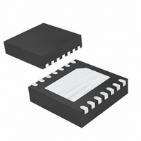
IC DAC 7BIT 2CH 5.5V 14-TDFN
Manufacturer
Maxim Integrated Products
Datasheet
1.DS4422NTR.pdf
(11 pages)
Specifications of DS4422N+T&R
Number Of Bits
7
Data Interface
I²C, Serial
Number Of Converters
2
Voltage Supply Source
Single Supply
Operating Temperature
-40°C ~ 85°C
Mounting Type
Surface Mount
Package / Case
14-TDFN Exposed Pad
Lead Free Status / RoHS Status
Lead free / RoHS Compliant
Power Dissipation (max)
-
Settling Time
-


NACK by transmitting a one during the ninth bit. Timing
for the ACK and NACK is identical to all other bit writes
(Figure 2). An ACK is the acknowledgment that the
device is properly receiving data. A NACK is used to
terminate a read sequence or as an indication that the
device is not receiving data.
Byte Write: A byte write consists of 8 bits of information
transferred from the master to the slave (most significant
bit first) plus a 1-bit acknowledgement from the slave to
the master. The 8 bits transmitted by the master are
done according to the bit-write definition, and the
acknowledgement is read using the bit-read definition.
Byte Read: A byte read is an 8-bit information transfer
from the slave to the master plus a 1-bit ACK or NACK
from the master to the slave. The 8 bits of information
that are transferred (most significant bit first) from the
slave to the master are read by the master using the
bit-read definition above, and the master transmits an
ACK using the bit write definition to receive additional
data bytes. The master must NACK the last byte read to
terminated communication so the slave will return con-
trol of SDA to the master.
Slave Address Byte: Each slave on the I
responds to a slave address byte sent immediately fol-
lowing a START condition. The slave address byte con-
tains the slave address in the most significant 7 bits
and the R/W bit in the least significant bit. The
DS4422/DS4424 slave address is determined by the
Two-/Four-Channel, I
Current DAC
Figure 2. I
8
TYPICAL I
START
A)
B)
EXAMPLE I
_______________________________________________________________________________________
SINGLE BYTE WRITE
-WRITE REGISTER
SINGLE BYTE READ
-READ REGISTER F8h
F9h TO 00h
MSB
2
A1
C WRITE TRANSACTION
2
2
C TRANSACTIONS (WHEN A0 AND A1 ARE GROUNDED)
C Communication Examples
A0
1
ADDRESS*
SLAVE
START
START
0
0
0 0 1 0 0 0 0 0
0 0 1 0 0 0 0 0
0
20h
20h
0
READ/
WRITE
R/W
LSB
SLAVE
SLAVE
ACK
ACK
SLAVE
ACK
1 1 1 1 1 0 0 1
1 1 1 1 1 0 0 0
MSB
F9h
F8h
b7
b6
REGISTER/MEMORY ADDRESS
2
SLAVE
SLAVE
C bus
*THE SLAVE ADDRESS IS DETERMINED BY ADDRESS PINS A0 AND A1.
b5
ACK
ACK
2
C, 7-Bit Sink/Source
b4
0 0 0 0 0 0 0 0
REPEATED
START
b3
b2
state of the A0 and A1 address pins. Table 1 describes
the addresses corresponding to the state of A0 and A1.
When the R/W bit is 0 (such as in A0h), the master is
indicating that it will write data to the slave. If R/W = 1
(A1h in this case), the master is indicating that it wants
to read from the slave. If an incorrect slave address is
written, the DS4422/DS4424 assume the master is com-
municating with another I
communication until the next START condition is sent.
Memory Address: During an I
master must transmit a memory address to identify the
memory location where the slave is to store the data.
The memory address is always the second byte trans-
mitted during a write operation following the slave
address byte.
Writing to a Slave: The master must generate a START
condition, write the slave address byte (R/W = 0), write
the memory address, write the byte of data, and gener-
ate a STOP condition. Remember that the master must
read the slave’s acknowledgement during all byte-write
operations.
Reading from a Slave: To read from the slave, the
master generates a START condition, writes the slave
address byte with R/W = 1, reads the data byte with a
NACK to indicate the end of the transfer, and generates
a STOP condition.
0 0 1 0 0 0 0 1
b1
SLAVE
ACK
21h
LSB
b0
STOP
SLAVE
ACK
SLAVE
ACK
MSB
b7
b6
DATA
b5
b4
DATA
MASTER
2
NACK
C device and ignore the
b3
I
2
2
C Communication
b2
C write operation, the
STOP
b1
LSB
b0
SLAVE
ACK
STOP
Related parts for DS4422N+T&R
Image
Part Number
Description
Manufacturer
Datasheet
Request
R

Part Number:
Description:
Two-/Four-Channel, I2C, 7-Bit Sink/Source Current DAC
Manufacturer:
MAXIM [Maxim Integrated Products]
Datasheet:

Part Number:
Description:
MAX7528KCWPMaxim Integrated Products [CMOS Dual 8-Bit Buffered Multiplying DACs]
Manufacturer:
Maxim Integrated Products
Datasheet:
Part Number:
Description:
Single +5V, fully integrated, 1.25Gbps laser diode driver.
Manufacturer:
Maxim Integrated Products
Datasheet:
Part Number:
Description:
Single +5V, fully integrated, 155Mbps laser diode driver.
Manufacturer:
Maxim Integrated Products
Datasheet:
Part Number:
Description:
VRD11/VRD10, K8 Rev F 2/3/4-Phase PWM Controllers with Integrated Dual MOSFET Drivers
Manufacturer:
Maxim Integrated Products
Datasheet:
Part Number:
Description:
Highly Integrated Level 2 SMBus Battery Chargers
Manufacturer:
Maxim Integrated Products
Datasheet:
Part Number:
Description:
Current Monitor and Accumulator with Integrated Sense Resistor; ; Temperature Range: -40°C to +85°C
Manufacturer:
Maxim Integrated Products
Part Number:
Description:
TSSOP 14/A�/RS-485 Transceivers with Integrated 100O/120O Termination Resis
Manufacturer:
Maxim Integrated Products
Part Number:
Description:
TSSOP 14/A�/RS-485 Transceivers with Integrated 100O/120O Termination Resis
Manufacturer:
Maxim Integrated Products
Part Number:
Description:
QFN 16/A�/AC-DC and DC-DC Peak-Current-Mode Converters with Integrated Step
Manufacturer:
Maxim Integrated Products
Part Number:
Description:
TDFN/A/65V, 1A, 600KHZ, SYNCHRONOUS STEP-DOWN REGULATOR WITH INTEGRATED SWI
Manufacturer:
Maxim Integrated Products
Part Number:
Description:
Integrated Temperature Controller f
Manufacturer:
Maxim Integrated Products
Part Number:
Description:
SOT23-6/I�/45MHz to 650MHz, Integrated IF VCOs with Differential Output
Manufacturer:
Maxim Integrated Products
Part Number:
Description:
SOT23-6/I�/45MHz to 650MHz, Integrated IF VCOs with Differential Output
Manufacturer:
Maxim Integrated Products
Part Number:
Description:
EVALUATION KIT/2.4GHZ TO 2.5GHZ 802.11G/B RF TRANSCEIVER WITH INTEGRATED PA
Manufacturer:
Maxim Integrated Products