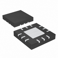
MAX5511ETC+ Maxim Integrated Products, MAX5511ETC+ Datasheet - Page 15

MAX5511ETC+
Manufacturer Part Number
MAX5511ETC+
Description
IC DAC 8BIT VOUT 12-TQFN-EP
Manufacturer
Maxim Integrated Products
Datasheet
1.MAX5510ETC.pdf
(18 pages)
Specifications of MAX5511ETC+
Settling Time
660µs
Number Of Bits
8
Data Interface
Serial
Number Of Converters
1
Voltage Supply Source
Single Supply
Operating Temperature
-40°C ~ 85°C
Mounting Type
Surface Mount
Package / Case
12-TQFN Exposed Pad
Resolution
8 bit
Interface Type
Serial (SPI)
Supply Voltage (max)
5.5 V
Supply Voltage (min)
1.8 V
Mounting Style
SMD/SMT
Supply Current
0.007 mA
Voltage Reference
Internal
Lead Free Status / RoHS Status
Lead free / RoHS Compliant
Power Dissipation (max)
-
Lead Free Status / Rohs Status
Lead free / RoHS Compliant
See Figure 3 for an illustration of how to power the
MAX5510/MAX5511 with either one lithium-ion battery
or two alkaline batteries. The low current consumption
of the devices makes the MAX5510/MAX5511 ideal for
battery-powered applications.
See the circuit in Figure 4 for an illustration of how to
configure the MAX5510 as a programmable current
source for driving an LED. The MAX5510 drives a stan-
dard NPN transistor to program the current source. The
current source (I
Figure 4.
Figure 3. Portable Application Using Two Alkaline Cells or One Lithium Coin Cell
Figure 4. Programmable Current Source Driving an LED
N
DAC
REFIN
IS THE NUMERIC VALUE OF THE DAC INPUT CODE.
I
LED
=
MAX5510
Applications Information
V
Programmable Current Source
REFIN
256 × R
0.1µF
DAC
______________________________________________________________________________________
LED
× N
DAC
+1.8V to +5.5V, Ultra-Low-Power, 8-Bit,
) is defined in the equation in
1.8V ≤ V
2.2V ≤ V
1-Cell and 2-Cell Circuit
ALKALINE
LITHIUM
REFERENCE)
(1µA, 1.25V
MAX6006
SHUNT
≤ 3.3V
≤ 3.3V
VOUT
FB
LED
536kΩ
V+
+1.25V
2N3904
R
I
LED
0.01µF
REFIN
MAX5510
See the circuit in Figure 5 for an illustration of how to con-
figure the MAX5510 to bias a current-output transducer.
In Figure 5, the output voltage of the MAX5510 is a func-
tion of the voltage drop across the transducer added to
the voltage drop across the feedback resistor R.
See the circuit in Figure 6 for an illustration of how to
use the MAX5511 to bias a two-electrode potentiostat
on the input of an ADC.
DAC
Figure 5. Transimpedance Configuration for a Voltage-Biased
Current-Output Transducer
REFIN
Voltage-Output DACs
V
GND
DD
MAX5510
V
BIAS
Voltage Biasing a Current-Output
DAC
TRANSDUCER
Self-Biased Two-Electrode
FB
VOUT
N
OF THE DAC INPUT CODE.
V
OUT
DAC
Potentiostat Application
=
IS THE NUMERIC VALUE
V
V
REFIN
OUT
I
T
256
(4.88mV / LSB)
× N
DAC
R
VOUT
N
OF THE DAC INPUT CODE.
V
BIAS
DAC
IS THE NUMERIC VALUE
=
V
REFIN
V
Transducer
OUT
256
× N
= V
BIAS
DAC
V
OUT
+ (I
T
× R)
15


